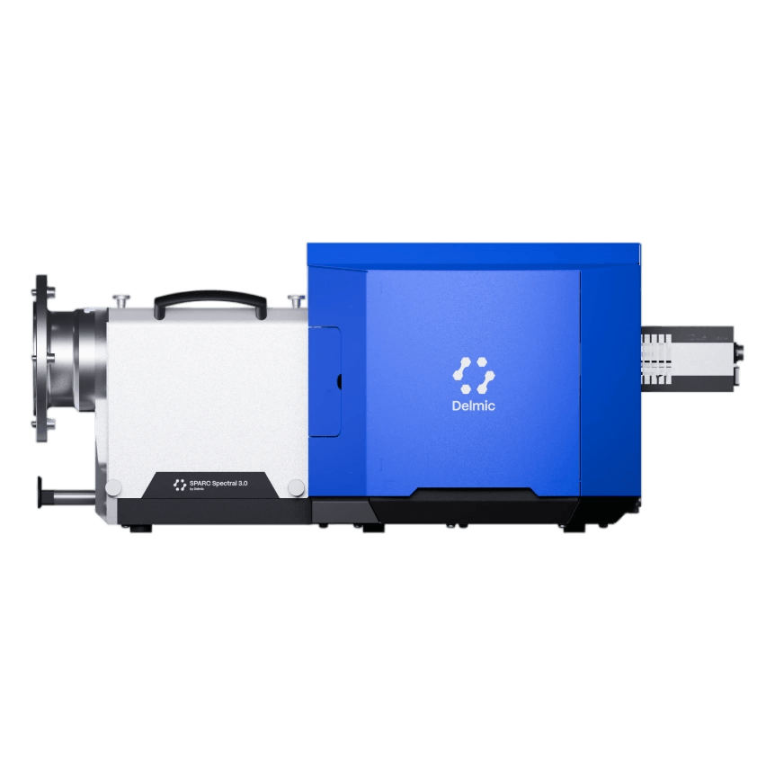
Cathodoluminescence Spectroscopy & Imaging
- Spectral and multi-mode CL analysis, specific modes depend on configuration
- Automated workflow to support data collection and analysis
- Modular design, optical and detection configurations can be selected according to research needs
Compact Cathodoluminescence Detector
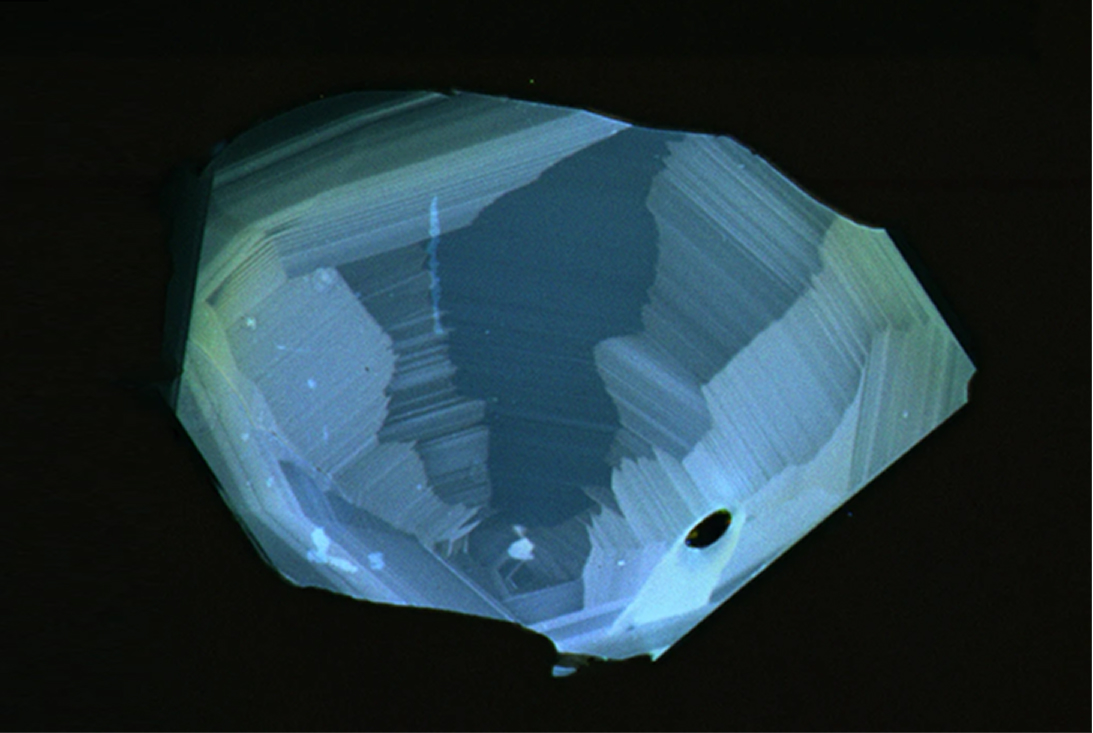
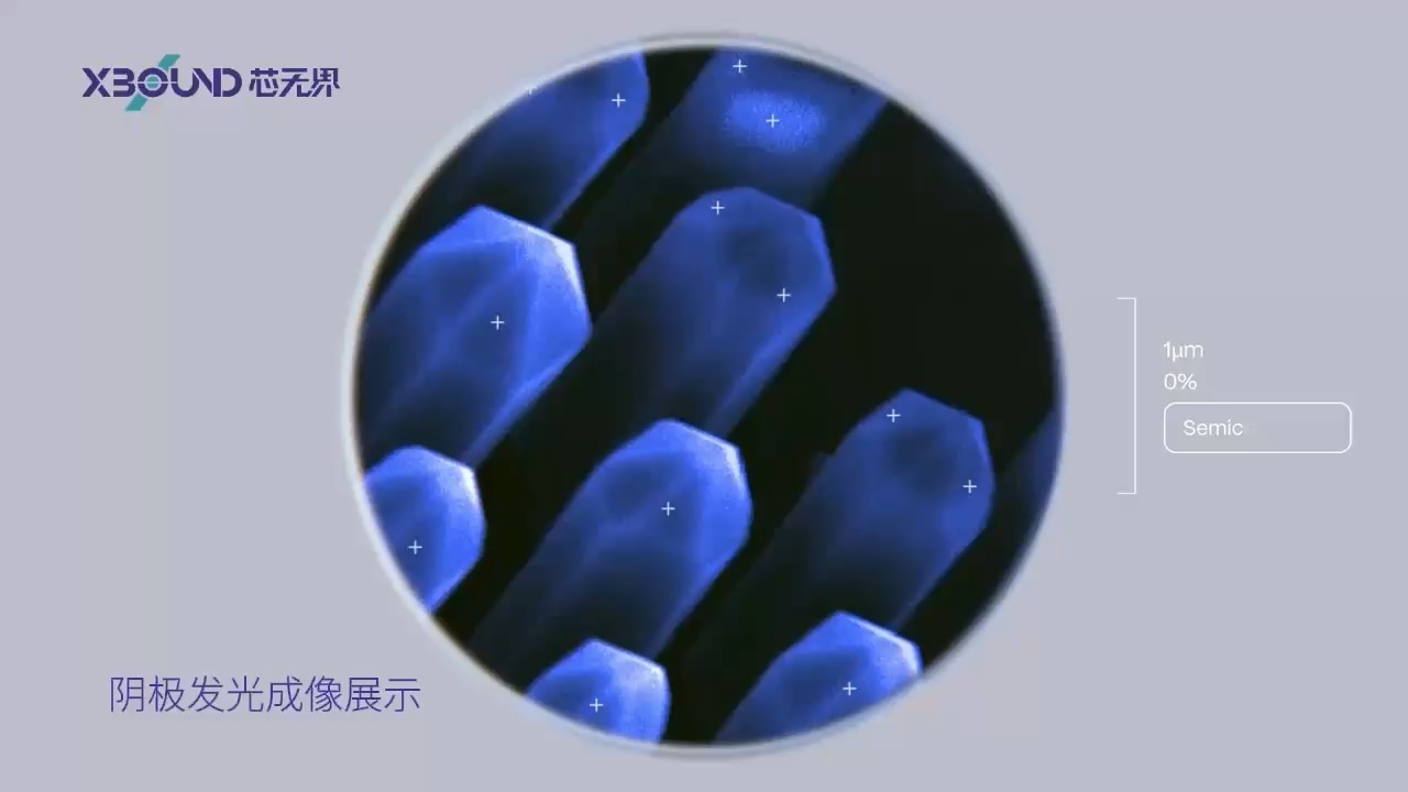
- Full color and filter intensity imaging to observe sample luminescence differences
- Combine SEM images to correlate microstructure and luminescence information
- Modular platform, upgrade capability is subject to specific configuration
Cathodoluminescence Intensity Detector
- Quickly start CL imaging without user alignment
- Full color imaging, RGB capability available as an option
- Supports correlation observation with other SEM signals, specific adaptation needs to be confirmed
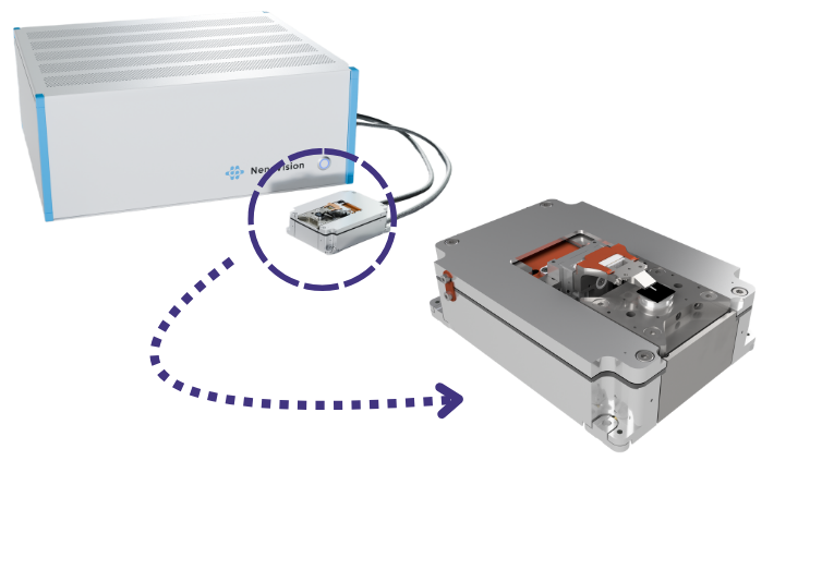
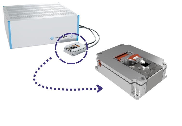
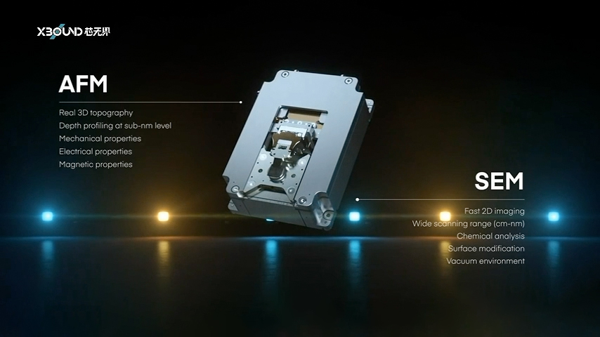
LiteScope AFM-in-SEM
- SEM navigation probe to locate areas of interest
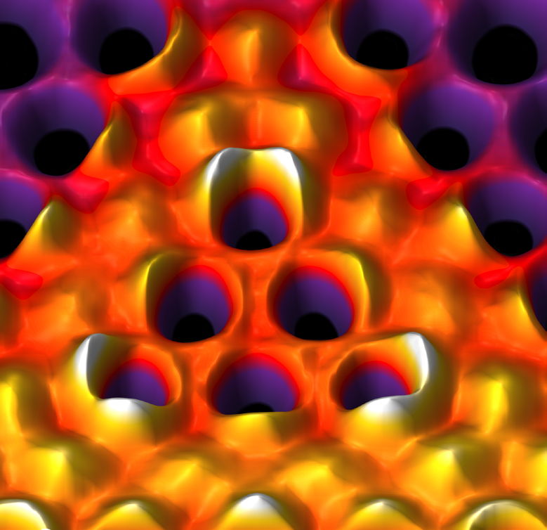
- AFM obtains the three-dimensional morphology of the surface and corresponding measurement information
- CPEM correlates SEM and AFM data;
- Measurement mode depends on probe, module and configuration
In-situ Laser Heating & Optical Excitation
- Localized laser acts on area of interest
- Support spot positioning and alignment
- Configure the experimental plan according to the scope, laser source and research needs
No products in this category yet. Contact our application engineers for advice.






 01










 021-3358 6350