




Applications | Cathodoluminescence for Microscopic Characterization
 |  |
 |  |
Cathodoluminescence (CL) Solution
Do you often fall into such a “physical toss”?
Measuring the morphology, looking at the composition, and analyzing the luminescence characteristics, the sample had to "string field" back and forth between several devices. This is not only time-consuming and labor-intensive, but also plagued by air pollution and surface oxidation, resulting in a significant reduction in the core "intrinsic luminescence" data.
How do you break down the invisible barriers between devices? Under the same vacuum environment, the multi-dimensional integrated characterization of a single product is realized, and Delmic gives the answer to the problem.
01| Selection of Nano Vacuum Interconnection Experiment Station
The Nano-Vacuum Interconnection Experiment Station NANO-X of the Suzhou Institute of Nanotechnology and Nano-Bionics chose to integrate the Delmic cathodoluminescence (CL) solution on the scanning electron microscope to build a "SEM + eds + CL" trinity characterization platform.
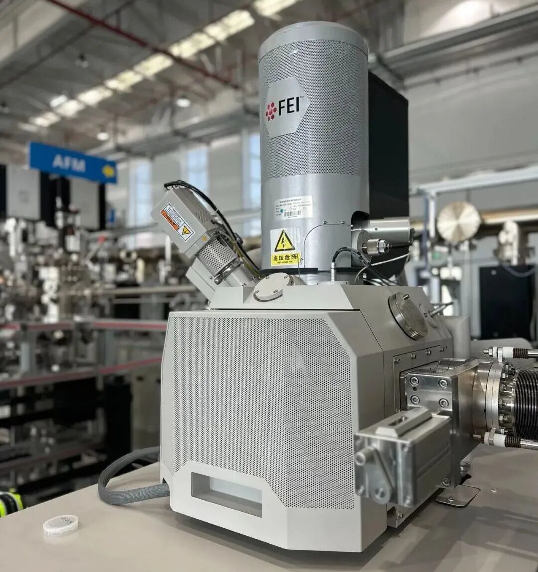
Figure 1 Nova Nano 450 scanning electron microscope with integrated Delmic CL solution at Suzhou Institute of Nanotechnology NANO-X (real shot)
Equipment model:Nova Nano 450-Delmic
As an important part of the country's major scientific and technological infrastructure, the nano-vacuum interconnection experimental station NANO-X interconnects material growth, processing and characterization equipment through ultra-high vacuum pipelines. When selecting models, the requirements for characterization are extremely stringent - both to ensure high resolution of imaging and component analysis, and to be able to obtain spectral information in situ in a vacuum environment. The Delmic CL protocol finally passed this test and became the core support for the platform's cathodic luminescence capabilities.
02| One system, three abilities
By integrating the Delmic CL solution, the system can simultaneously perform three types of characterization tasks:
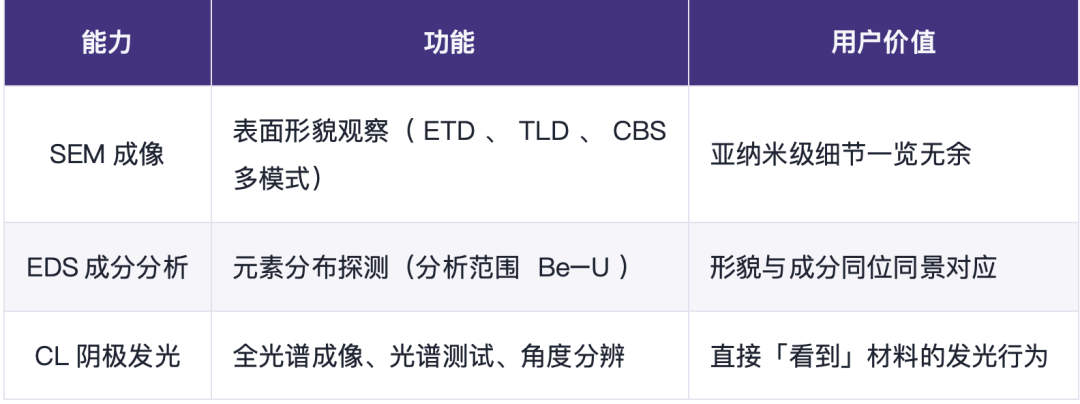
SEM + eds + CL Trinity Characterization Platform
It is no longer necessary to transport samples between multiple instruments, and the correlation analysis of morphology-component-luminescence can be completed in one injection.
Delmic × XBOUND Free Test Service
03| Hardcore Indicator: Measure microscopic limits with data
In the imaging mode, the scheme provides three options: rapid imaging supports large-scale, full-band or single-band luminescence imaging, which is suitable for batch screening of semiconductor and mineral samples; hyperspectral imaging works at a spectral resolution of better than 0.1 nm in the 185-900 nm wavelength range, revealing the local optical and structural characteristics of nanomaterials; and angular resolution mode outputs angular profile information, which characterizes the material properties according to the directionality of luminescence, which is of great value in the field of nanophotonics.
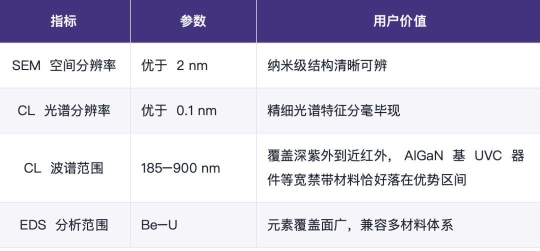
Protocol Core Metrics: Spectral Resolution, Wavelength Range, and Detection Configuration
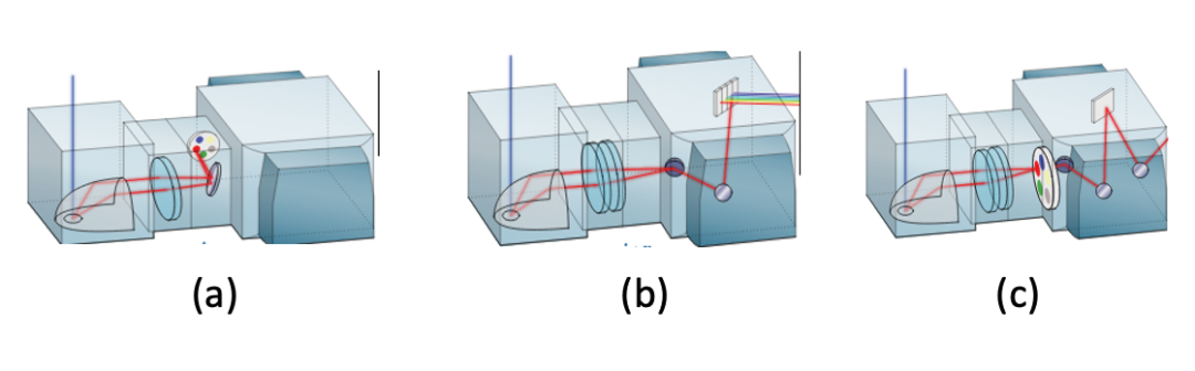
Figure 2 Schematic diagram of the optical paths of the three imaging modes of CL: (a) rapid imaging; (b) hyperspectral imaging; and (c) angle resolution
04| Delmic Scenarios
In the vacuum interconnection system of NANO-X, the value of this integration scheme is further amplified:
Growth — characterizing interconnections:After the film is grown, it enters the characterization cavity directly through the vacuum pipeline, avoiding the interference of air, water vapor and impurities on the morphology, energy spectrum and luminescence characteristics, and measuring the true state of the material "just out of the furnace".
Process — Test Connection:In conjunction with etching and other process equipment, the surface oxide layer and contamination layer can be removed first, and then the intrinsic luminescence and element distribution of the sample can be measured.
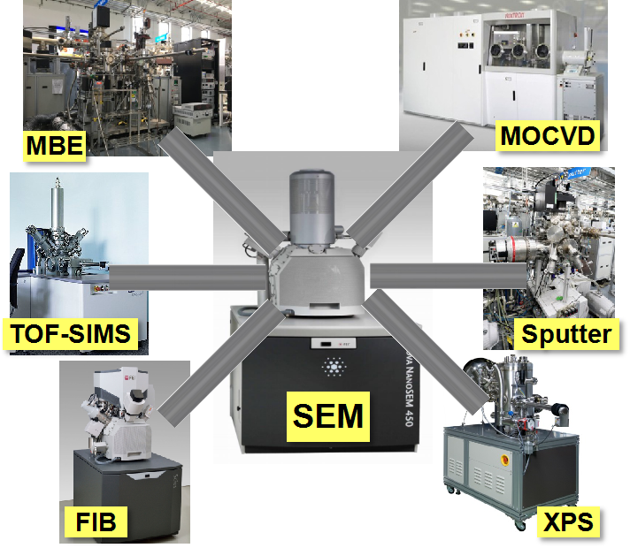
Figure 4 NANO-X vacuum interconnection layout: SEM interconnection with MBE, MOCVD, FIB, XPS, TOF-SIMS, Sputter and other devices
This is what distinguishes the Delmic CL protocol from regular offline testing: it not only adds a feature, but it reshapes the research paradigm of growth-characterization.
05| Thesis Demonstration: Equipment Cases
Around this platform, Suzhou Nano Institute and its collaborative team have produced a number of high-level research results:
Component Diffusion Analysis (SEM-EDS)
Using the eds Mapping function, the composition diffusion behavior at the interface between β- (AlxGa1-x) 2O3 film and β-Ga2O3 was revealed. The results were published in Physica Status Solidi A (2021) under the title "Bandgap Tailoring of Monoclinic Single-Phase β- (AlxGa1-x) 2O3 (0 ≤ x ≤ 0.65) Thin Film by Annealing β-Ga2O3/Al2O3 Heterojunction at High Temperatures".
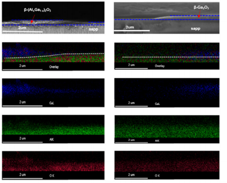
Figure 5 eds Mapping reveals component diffusion at the interface between β- (AlxGa1-x) 2O3 and β-Ga2O3 (Phys. Status Solidi A, 2021)
Polar Structure Characterization (SEM-CL)
Aiming at the lateral polarity structure of AlGaN material system on sapphire substrate, the morphology was combined with luminescence by CL line scanning, the optical properties of group III polar domain and N polar domain were comparatively studied, and the effect of substrate nitriding treatment on the polarity control of UVC AlGaN-based multi-quantum wells was investigated. The results were published in ACS Applied Nano Materials (2020).
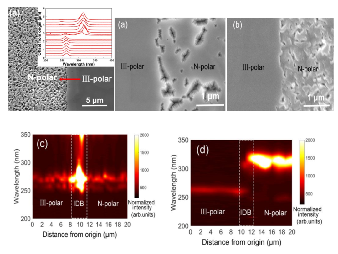
Figure 6 SEM-CL Comparison of morphology and luminescence distribution of AlGaN lateral polar structure of sapphire substrate (ACS Appl. Nano Mater., 2020)
Heterojunction Defect Analysis (SEM-CL)
All-optical imaging was performed on the GaInP/Si heterojunction cross-section grown by HVPE epitaxy to compare the luminescence difference between the doped and undoped regions, and the doping concentration was calculated from the spectrum. The results were published in the Journal of Applied Physics (2020, 128, 055308).
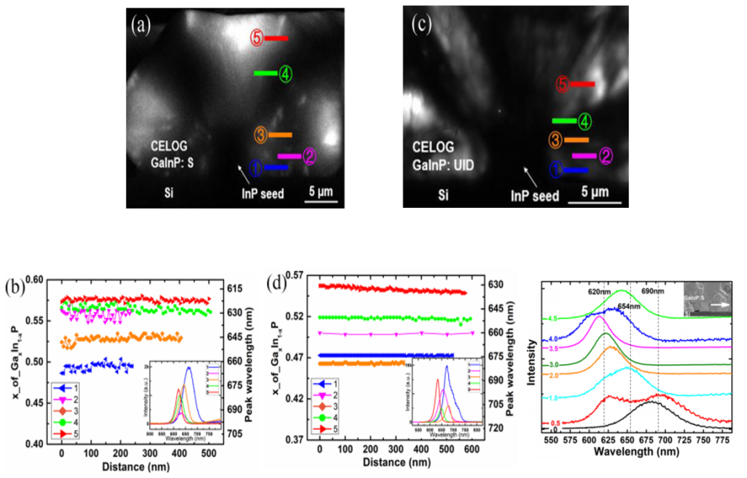
Figure 7 CL all-optical imaging and spectroscopy of GaInP/Si heterojunction cross-section: S-doped versus un-doped region luminescence (J. Appl. Phys., 2020)
From Group III nitrides to gallium oxide to III–V/Si heterojunctions, the Delmic CL protocol has yielded solid answers in different material systems.
06| Delmic 3.0 Highlights
Eight powerful imaging modes
The Delmic cathodoluminescence solution is modular in design, enabling multi-dimensional experiments in a single system. Compared with version 2.0, the new 3.0 solution adds monochrome imaging and light excitation modes, making it more powerful.
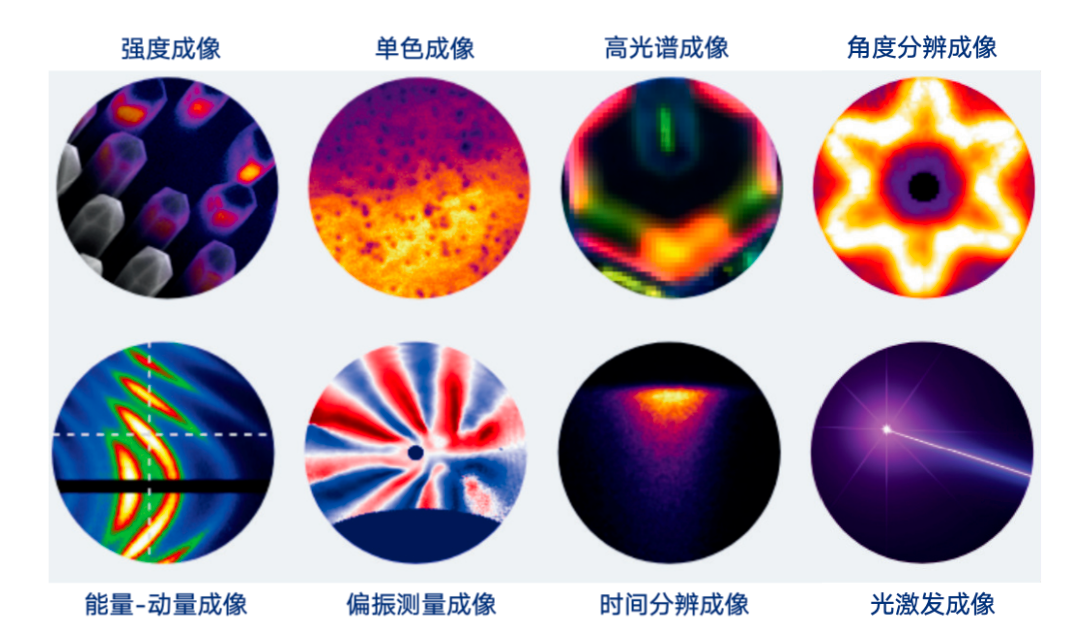
Delmic 3.0: Eight powerful imaging modes
2.3x faster hyperspectral scanning
CCD hardware triggered, 128 × 128 pixel scan reduced from 15.4 minutes to 6.5 minutes. Beam-sensitive samples can be scanned for higher resolution before degradation.
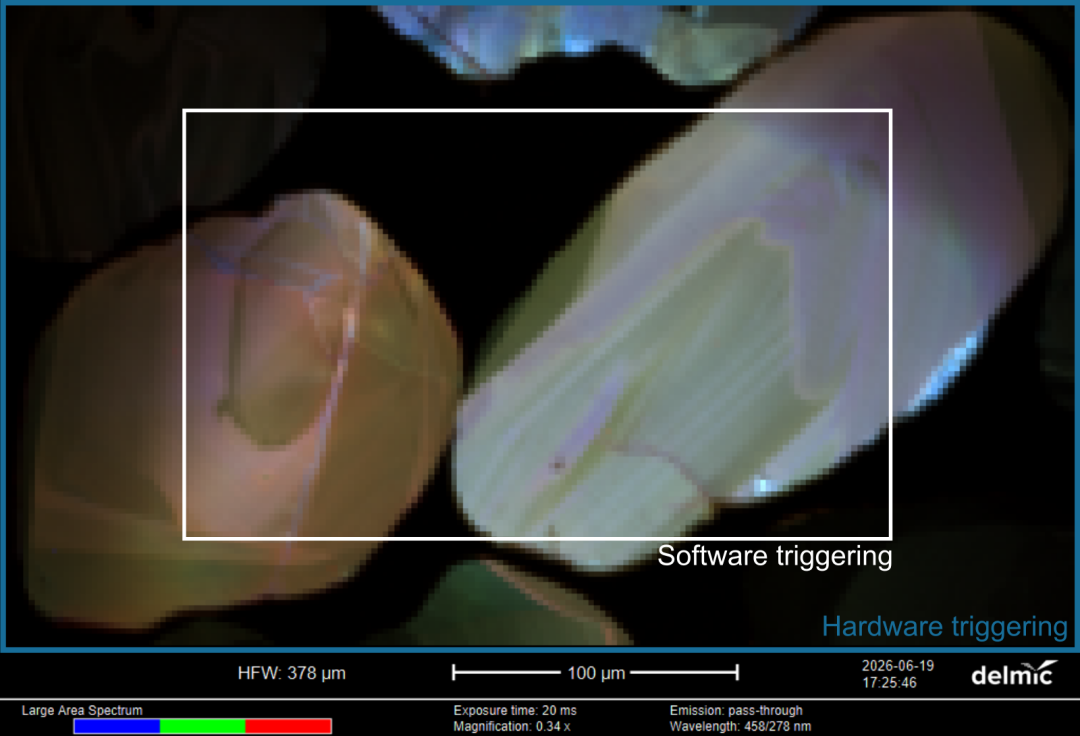
ODEMIS software acquisition interface (CCD hardware trigger)
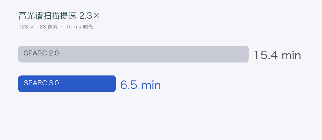
Hyperspectral scan speed-up: 15.4 minutes → 6.5 minutes
07Why Choose Us?
Delmic focuses on cathodoluminescence and light-emitting electron microscopy solutions. Its CL system is known for its high spectral resolution, wide spectral range and flexible imaging modes, and has served many scientific research institutions and platforms around the world.
As a Delmic China agent, XBOUND provides domestic users with full process localization support from selection consulting, installation training to application method development. Whether your project involves wide bandgap semiconductors, nanophotonics or photovoltaic materials, we can tailor the SEM-CL characterization scheme to your needs.
Delmic Cathodoluminescence Technology Series Products
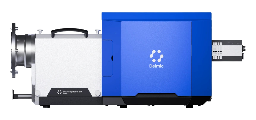
SPARC Spectral 3.0
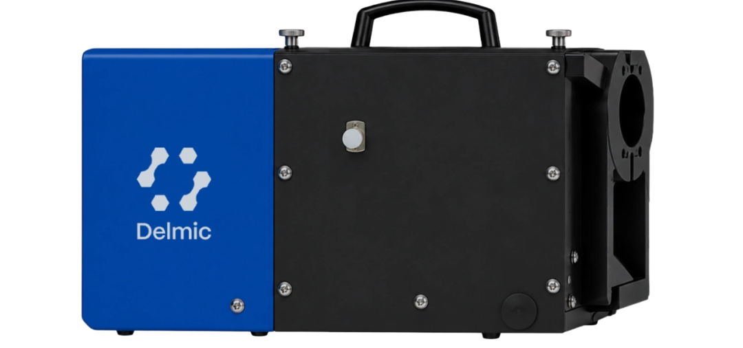
SPARC Compact
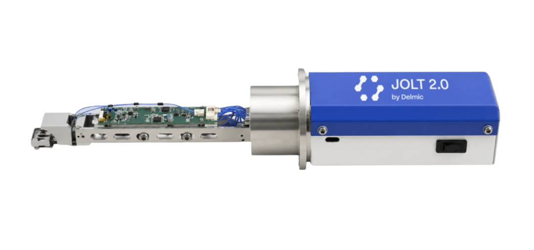
JOLT
Related Reading: Breaking Down Technical Barriers! The new generation of the flagship cathodoluminescent system SPARC Spectral 3.0 has been released (see Issue 05 of this document).
Consultation Hotline: 021-3358 6350 | E-mail:info@xbound-tech.com
XBOUND Characterization Technology is committed to exploring the microscopic world boundaries, focusing on advanced electron microscopy and multi-dimensional characterization technology. Through innovative instrument platforms and professional solutions, electronic microscopy, in-situ analysis, photoelectric correlation and intelligent characterization technologies are connected, providing unlimited possibilities for scientific research and industrial innovation.At present, we mainly provide the following products: advanced SEM/TEM accessories such as Delmic cathodoluminescence in the Netherlands, NenoVision electron microscope atomic force microscope in the Czech Republic, and Waviks in-situ laser heating and light excitation system in the United States. At present, there is a demo experience center in Shanghai, and after-sales service covers the whole country.


Scan the code to focus on "XBOUND Characterization Technology"
 021-3358 6350