




Hello, We're Here! Explore the Microscopic World with XBOUND
 |  |
 |  |
The microscopic world begins with “seeing”
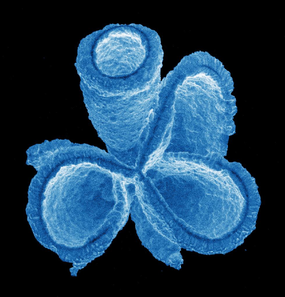
Electron microscopy is an indispensable tool for people who study the microscopic world. Under the lens, we can touch more details, such as the shape of the material, structure, defects, etc., which can be observed, recorded and analyzed.
But “seeing” is never just the beginning of exploration.
As research deepens, people are no longer content with just that, but want to know why the world is the way it is, how change happens, and what we can change.
This is why we focus on advanced electron microscopy and multi-dimensional characterization techniques.
Exploring the unknown is more than “seeing”
As demand grows, so do traditional ways of looking. The development of advanced SEM/TEM accessories and multi-dimensional characterization technology has provided us with more possibilities for observation and research.
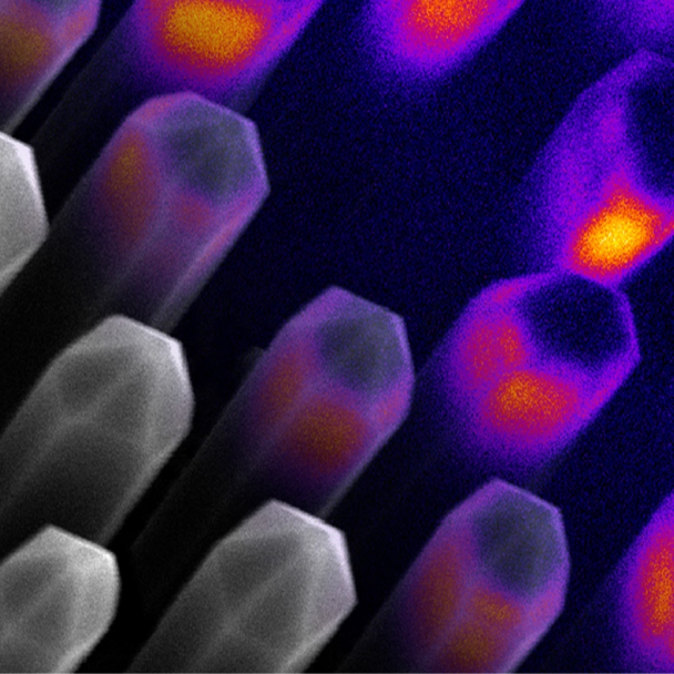
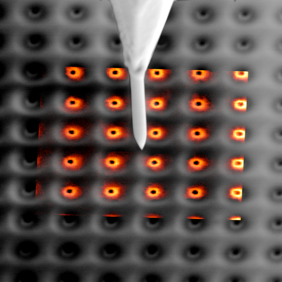
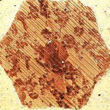
XBOUND introducedDelmic Cathodoluminescence、NenoVision Electron Microscope Atomic Force Microscope、Waviks in-situ laser heating and light excitation systemand other advanced microscopic characterization techniques, while also supporting the integration of practical application needsDomestic customizationEquipment and solutions, hoping to provide richer and more flexible technology options for different research directions and experimental needs.
Through these evolving characterizations, researchers can further observe, record, and analyze changes in the microcosm in specific environments, during changes in the sample, or when different conditions are applied to the sample.
Each new technique, each new characterization, is helping researchers move further into the unknown.
Expand, not just more
For us, the value of a product is more than just adding a new feature. We are more concerned about how to integrate new technologies into existing research work, how to approach the same problem from different angles, and provide more technical support for new research directions.
From the initial application communication to the selection of solutions based on actual needs; from product selection to follow-up technology and after-sales service, we hope to accompany users to complete the entire process from demand to application.
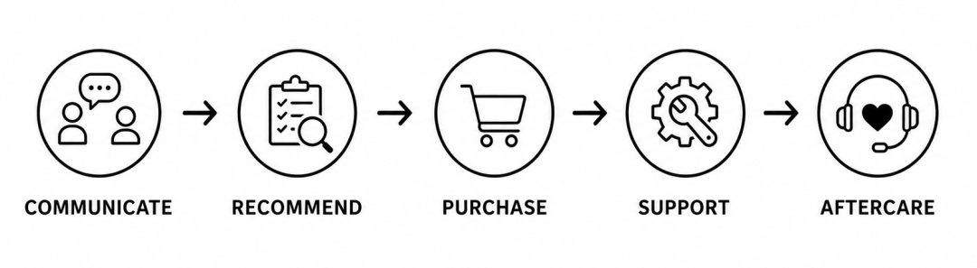
Whole process service: communication, → recommendation, → purchasing → support, → after-sales service
We believe that truly professional service is not a simple product delivery, but a professional and continuous support for users throughout the process.
It's a pleasure to meet you all from here
This is where we begin.
In the future, we will continue to focus on advanced SEM/TEM and multi-dimensional characterization technology, focusing on more possibilities brought about by the expansion of SEM/TEM functions. By introducing advanced products, providing professional application support and continuous service, while combiningDomestic customizationDevices and solutions, we want to be closer to the actual needs of different users and explore the micro-world with more researchers.
We want to be a trusted professional partner as you explore advanced microscopic characterization techniques.
Hi microscopic world, here we come!
XBOUND products
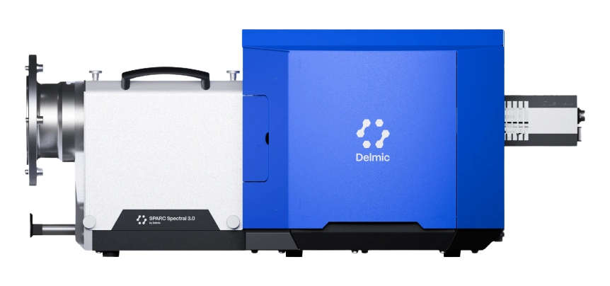
Delmic Cathodoluminescence
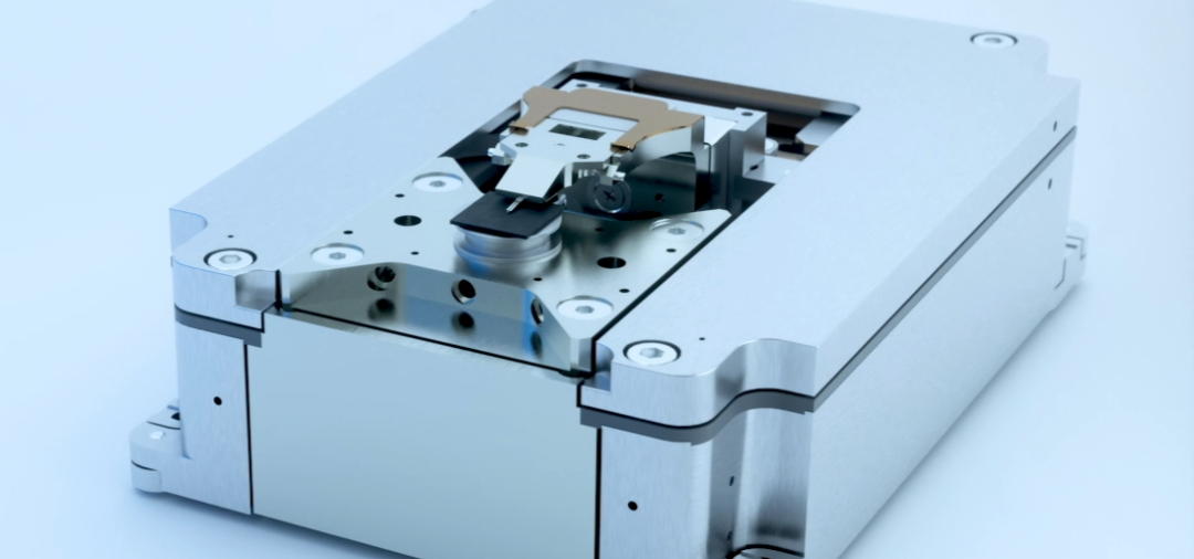
NenoVision Electron Microscope Atomic Force Microscope
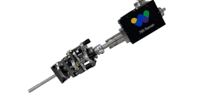
Waviks in-situ laser heating and light excitation system
Hotline: 8621-3358 6350
XBOUND Characterization Technology is committed to exploring the microscopic world boundaries, focusing on advanced electron microscopy and multi-dimensional characterization technology. Through innovative instrument platforms and professional solutions, electronic microscopy, in-situ analysis, photoelectric correlation and intelligent characterization technologies are connected, providing unlimited possibilities for scientific research and industrial innovation.At present, we mainly provide the following products: advanced SEM/TEM accessories such as Delmic cathodoluminescence in the Netherlands, NenoVision electron microscope atomic force microscope in the Czech Republic, and Waviks in-situ laser heating and light excitation system in the United States. At present, there is a demo experience center in Shanghai, and after-sales service covers the whole country.


Scan the code to focus on "XBOUND Characterization Technology"
 021-3358 6350