




XBOUND invites you to the 2026 National Electron Microscopy Annual Conference
 |  |
 |  |
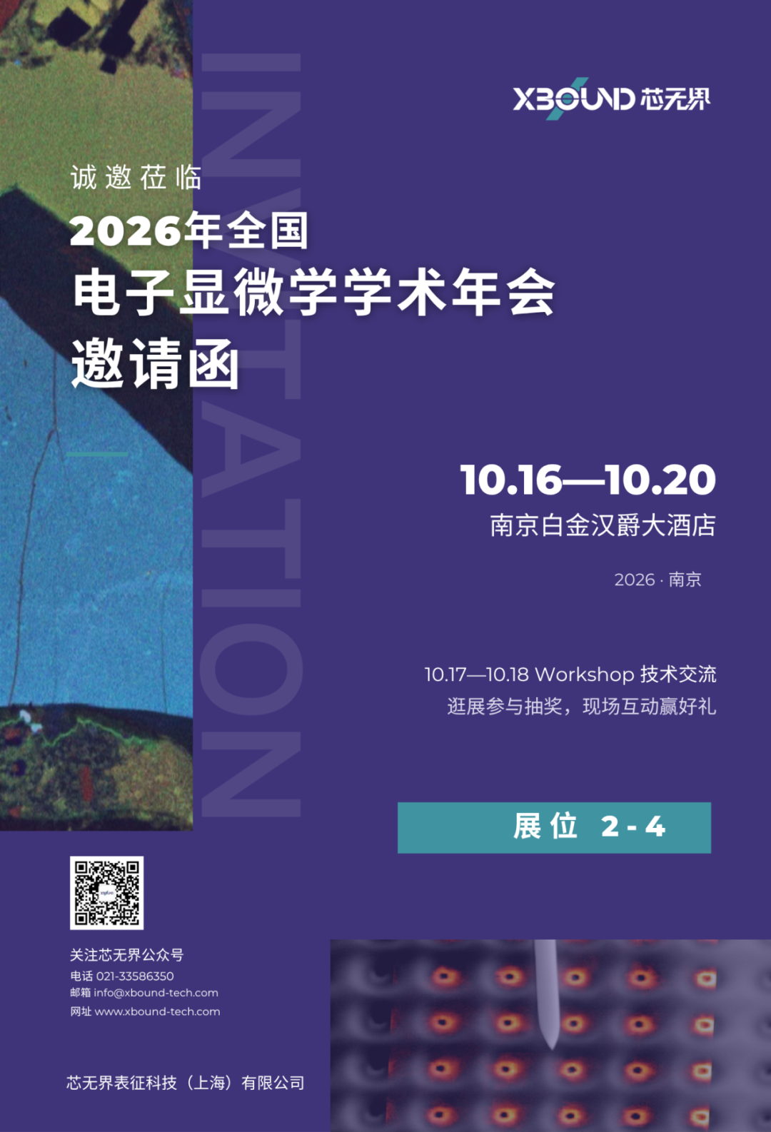
2026 National Electron Microscopy Annual Conference · Conference Invitation (Nanjing Buckingham Hotel · Booth 2-4)
On October 16—20, 2026, the 2026 National Electron Microscopy Annual Conference will be held at the Buckingham Grand Hotel in Nanjing. This year coincides with the 100th birthday of Mr. Qian Linzhao, founder of China's electron microscopy. The theme of this annual conference is "microscopic dislocation, weaving microscopic warp and weft; centuries of inheritance, continuing to write the legend of the stars". There are 16 special sessions, gathering microscopists at home and abroad.
XBOUND XBO
Meeting Date:October 16 - 20, 2026
Meeting location:Buckingham Grand Hotel (Nanjing Branch)
Booth #:2-4
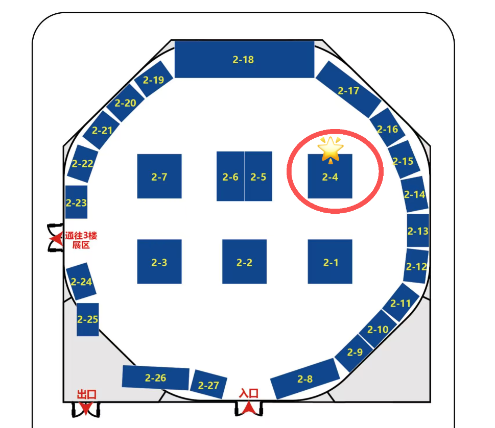
Booth Plan: Booth 2-4 Location Schematic
Booth # 2-4
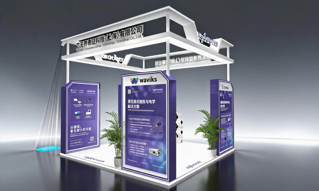
XBOUND booth renderings
Whether it is metal matrices such as aluminum, magnesium, and titanium alloys, or non-metallic matrices such as resins, ceramics, carbon, and even various types of reinforcing fibers, behind the rapid development of life sciences and high-end manufacturing, it is the ultimate inquiry into macro performance and microstructure.
Scanning electron microscopy helps you solve imaging problems, but real research and failure analysis problems often need to see its composition, physical properties, and how it changes under what conditions. XBOUND brings you multiple, multi-dimensional solutions such as Delmic cathodoluminescent CL, NenoVision AFM-in-SEM electron microscope atomic force microscope, Waviks in-situ photothermal and spectroscopic analysis system, and Technoorg Linda argon ion sample series.
Cathodoluminescent (CL) series
As a leader in advanced electron microscope accessories, the Delmic cathodoluminescence detection system can be seamlessly adapted to various types of scanning electron microscopes (SEMs), combining the light signal excited by electron beams with the microstructure of materials to provide high-resolution cathodoluminescent image characterization solutions for wide bandgap semiconductor, photoelectric devices, materials science and geological science research.
Recommended model
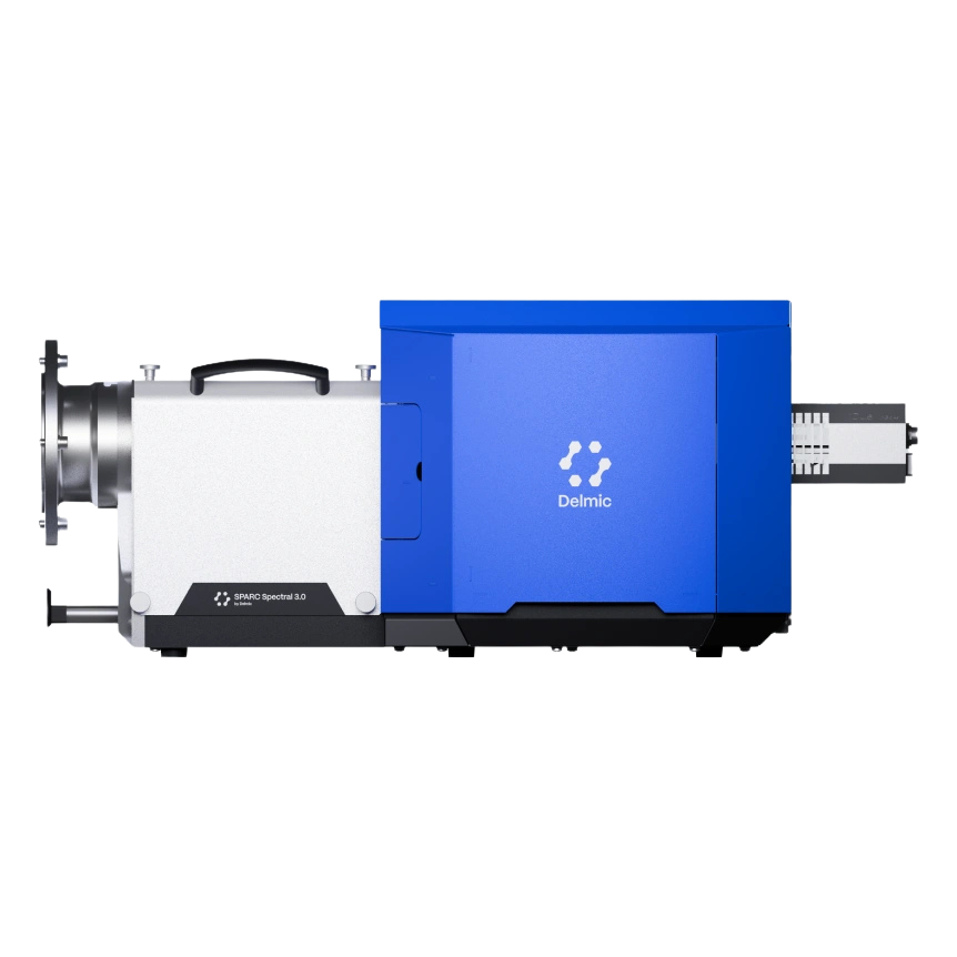
SPARC Spectral 3.0 Spectral CL System
Location:Full-featured, high-end research-grade system.
Core features:Integrated spectrum and imaging to accurately correlate the emission spectrum with the position of the sample, covering a band of 185—1700 nm.
Skills Needed:It is suitable for defect luminescence, structural difference analysis, and supports a variety of measurements such as hyperspectral, angular resolution, polarization, and time resolution.
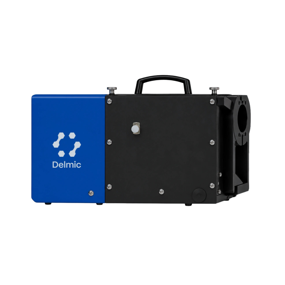
SPARC Compact High Performance cathodoluminescence Detector
Location:Highly flexible, versatile standard system.
Core features:The modular design supports fast full-band and color filtering to easily generate realistic RGB color or pseudo-color images.
Skills Needed:Widely used in multi-band imaging analysis of semiconductor defects, geological minerals (such as zircon ring), etc.
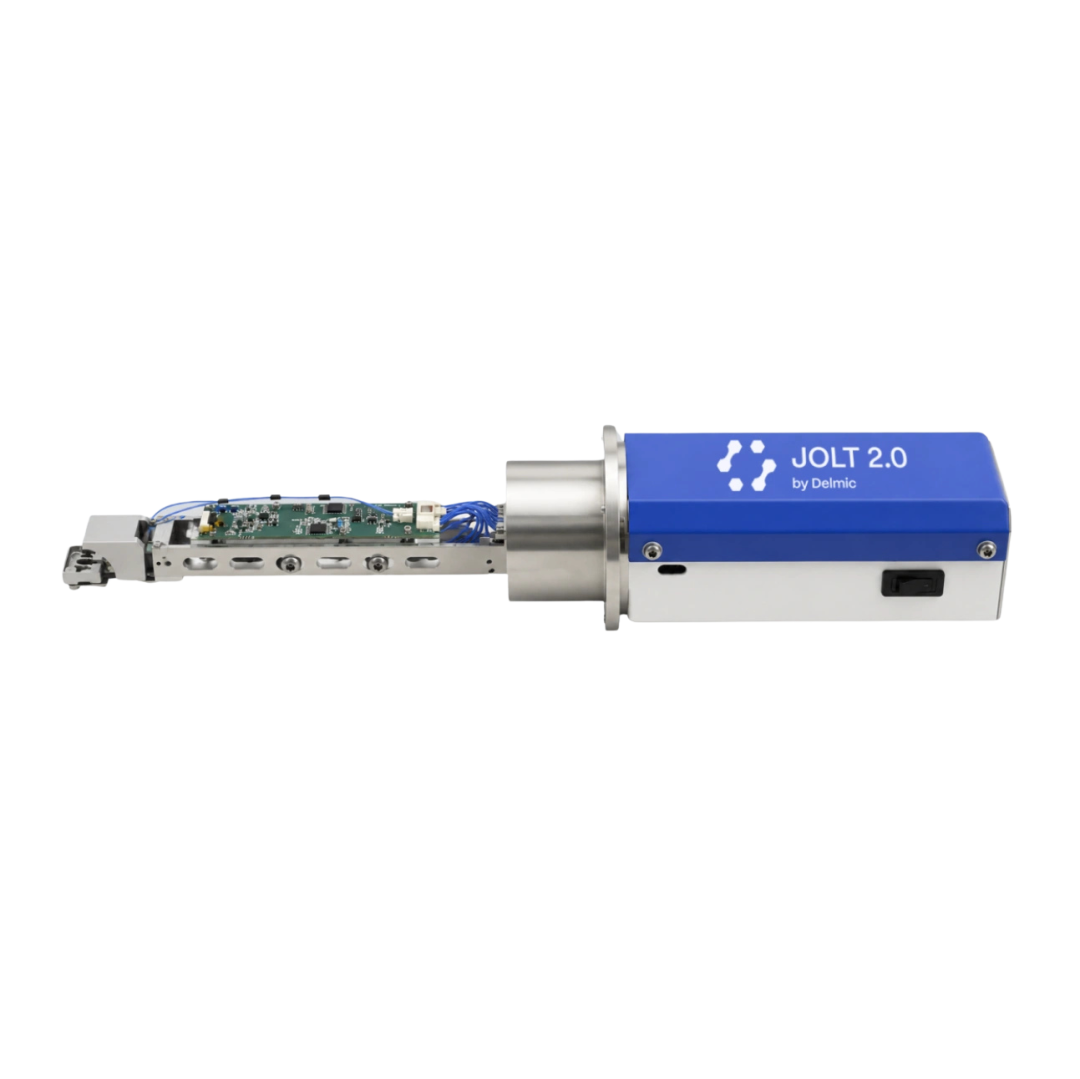
Jolt entry level cathodoluminescence detector
Location:Efficient, easy-to-use rapid screening tool.
Core features:Compatible with all scanning electron microscopes, supports panchromatic and RGB imaging, field of view exceeds 10 mm ², calibration-free and large-area synchronous acquisition.
Skills Needed:Especially suitable for rapid macroscopic CL imaging and pretreatment of ceramics, geological samples and semiconductors for efficient screening.
Application cases
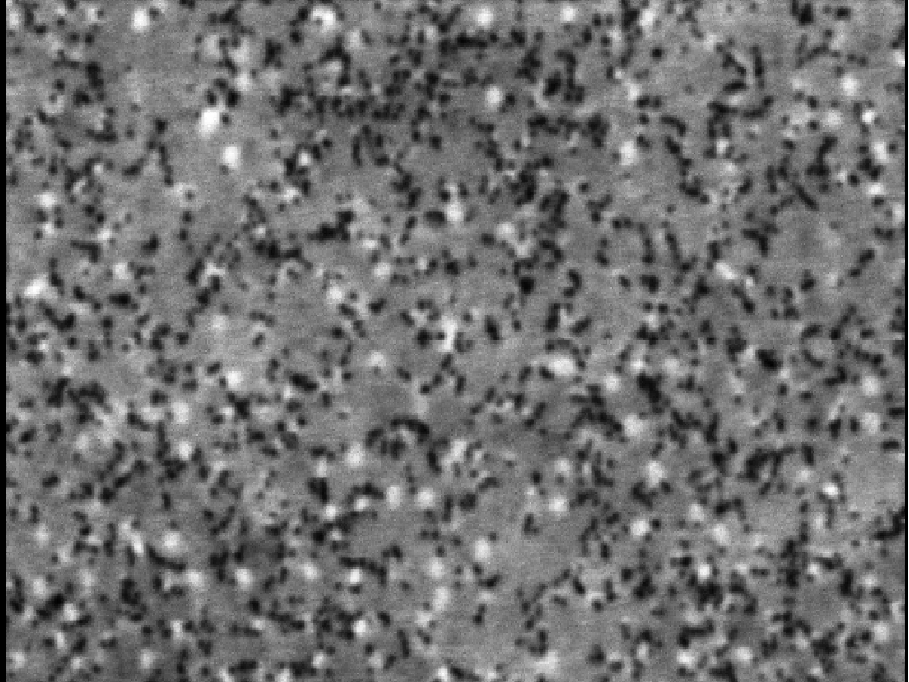
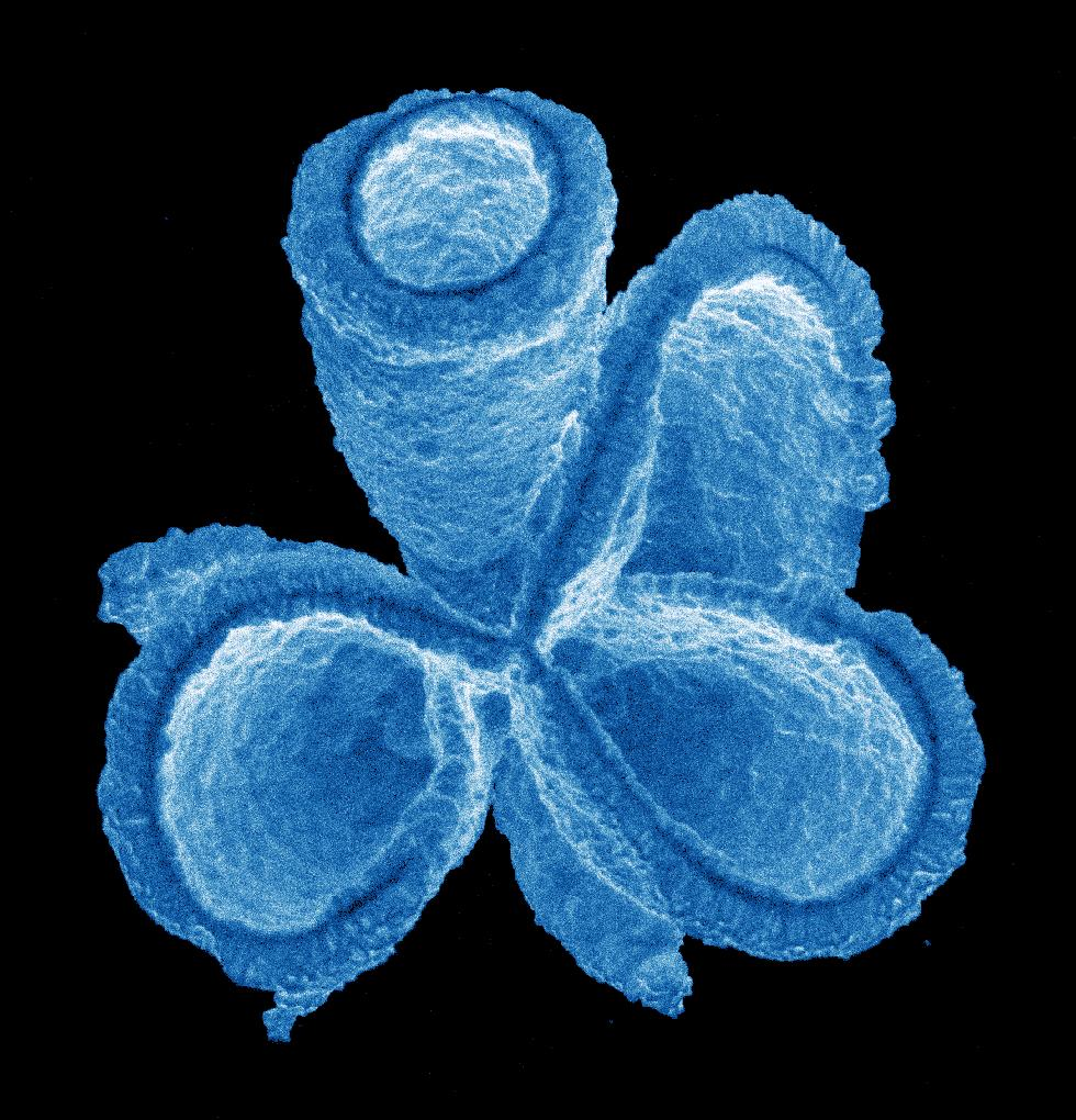
Monochrome CL image penetrating dislocations in InGaN MQW (LED on silicon substrate)
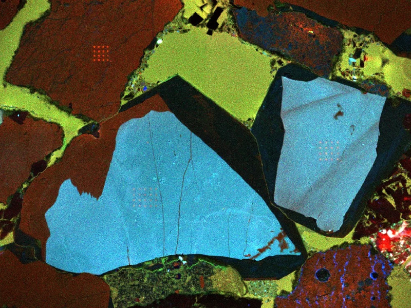
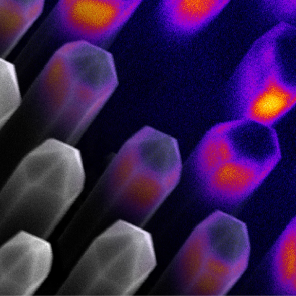
RGB CL strength of quartz sandstone
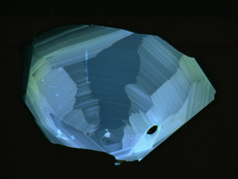
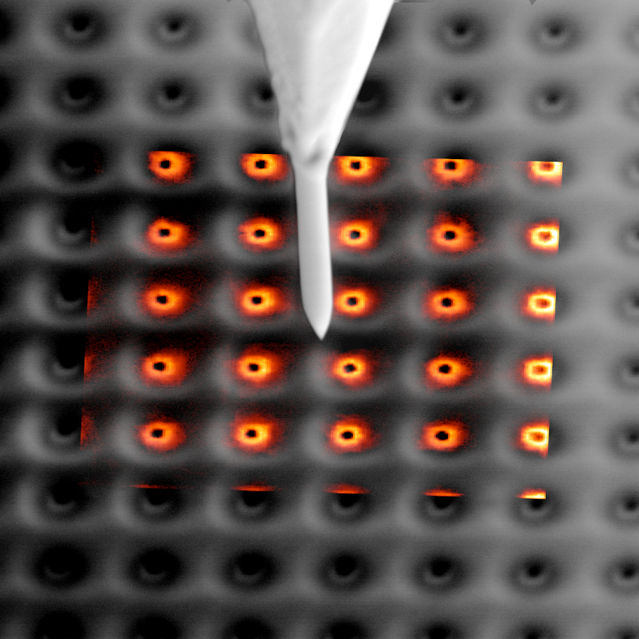
Zircon CL luminescence imaging
Electron microscope atomic force microscope
The LiteScope Atomic Force Microscope (AFM-in-SEM) is an in-situ multimodal correlation analysis system designed for scanning electron microscopy (SEM). It can be seamlessly embedded in the mainstream SEM cavity, and the AFM and SEM data can be synchronized in the same environment and position by accurately positioning the probe from the real-time viewing angle of the electron microscope. The system is widely used in materials science and nanotechnology, semiconductors and micro and nanoelectronic devices, life sciences and biomedicine, and energy, energy storage and catalysis research.
Recommended model
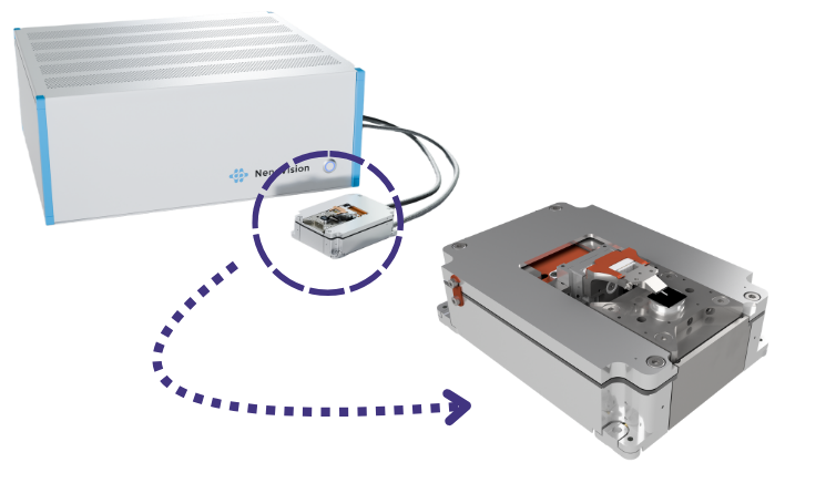
LiteScope Electron Microscope Atomic Force Microscope
Precise navigation at the micron level:AFM probes are precisely positioned using a scanning electron microscope (SEM) real-time viewing angle to achieve high-resolution morphology imaging at the micron to nanometer level.
Multi-modal sync associations:According to the probe and module configuration, conductivity, surface potential, mechanics, magnetics and piezoelectric analysis can be expanded, conductivity, surface potential, mechanics, magnetics and piezoelectric domain analysis can be expanded, and the virtual electrode can be simulated by an electron beam instead of the traditional physical back contact, making it possible to measure the C-AFM and SSRM of the substrate non-conductive sample, providing multi-dimensional information in the same position for semiconductor microstructure and failure analysis.
Full-featured mode:C-AFM, SSRM, KPFM, EFM, PFM, MFM, I-V curve, F-z curve and electron beam virtual electrode C-AFM.
Broad system compatibility:Deeply adapts to mainstream scanning electron microscope brands, and supports customized cavity and hardware integration to meet diverse scientific research and industrial characterization needs.
Application cases
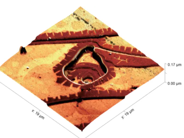
SEM precise positioning + AFM topography + 3D correlation
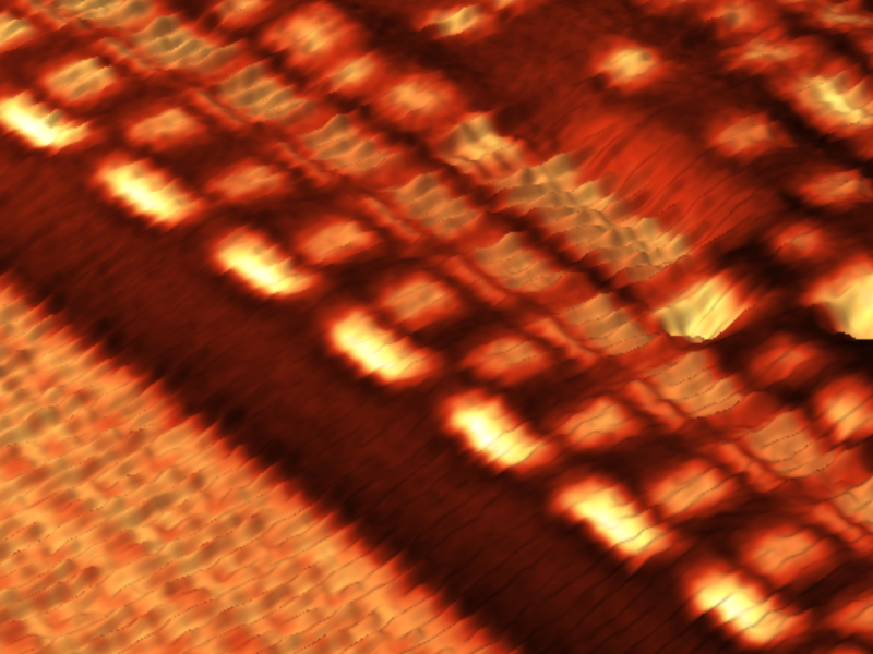
De-tiering SEM/AFM association
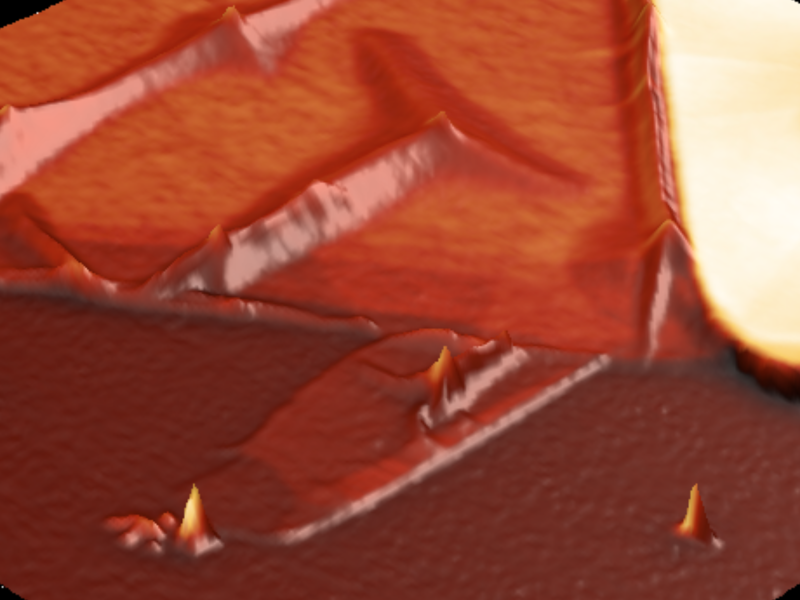
WSe2 Nanopillar SEM/AFM Association
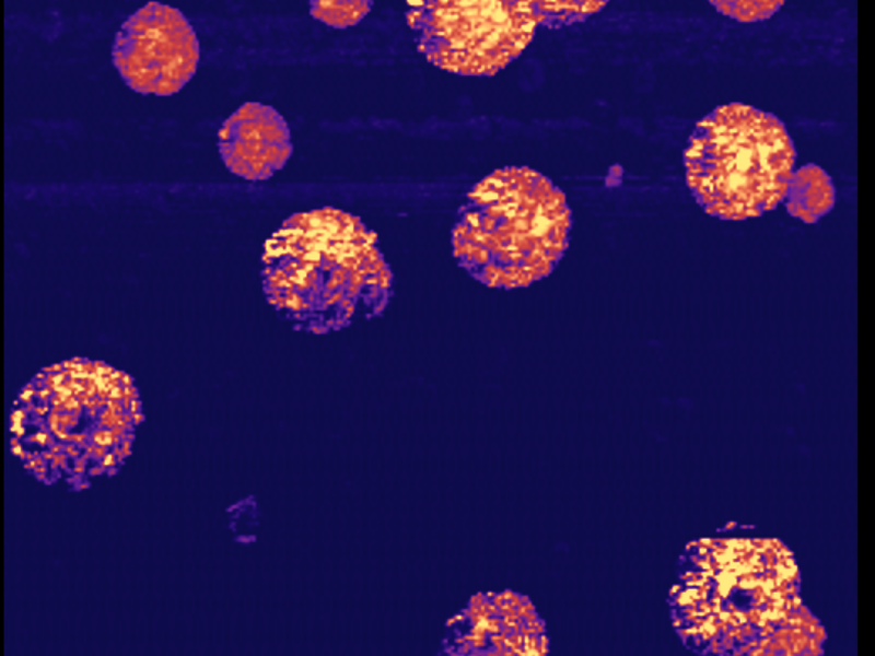
Characterization of micro-nano-Si structure
In-situ photothermal and spectroscopic analysis system
As an innovator in the field of micro- and nano-scale photothermal characterization and in-situ physical testing, Waviks is committed to expanding multi-dimensional in-situ excitation and analysis capabilities for scanning electron microscopy (SEM).
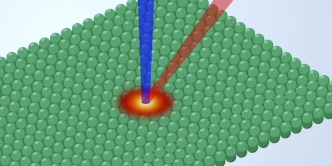
Aiming at the thermal/optical failure problems of third/fourth generation semiconductors (GaN, SiC, gallium oxide, diamond, etc.), micro-nano photoelectric devices, and advanced packaging, Waviks Vesta integrates high-precision local optical excitation, laser in-situ heating, and related spectral analysis depth seamlessly into the electron microscope cavity.
The system upgrades the traditional static morphology observation electron microscope to a dynamic physics experimental platform, which can efficiently carry out micro-area photoelectric response analysis, laser annealing process simulation, FIB ion beam damage repair, and in-situ characterization of thermal stress evolution at the nanoscale, providing a strong microscopic mechanism support for semiconductor material research and development and failure analysis.
Recommended model
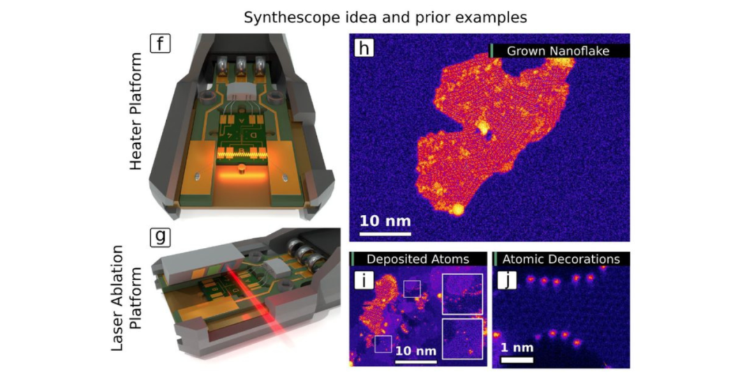
Vesta TEM Edition
Compatible with all TEM brands and models
Compatible with all eds geometries
Mirrors tailored for small pole shoe clearance
Tunable laser source for precise phonon coupling
Precision in-situ nanofabrication at the atomic level
EEGS/sEELS for quantum material characterization
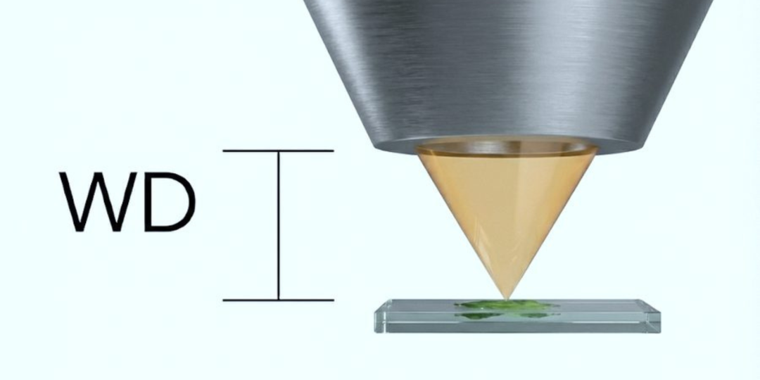
Vesta Full Size SEM/FIB Edition
Includes all desktop SEM features, plus:
Fully automatic three-dimensional nano manipulator
Pulsed laser photon bombardment enhanced etching
Electron Beam Induced Deposition (EBID) Purification
Compatible with Ga FIB, PFIB, He ion FIB
Laser-assisted applications during ion beam grinding
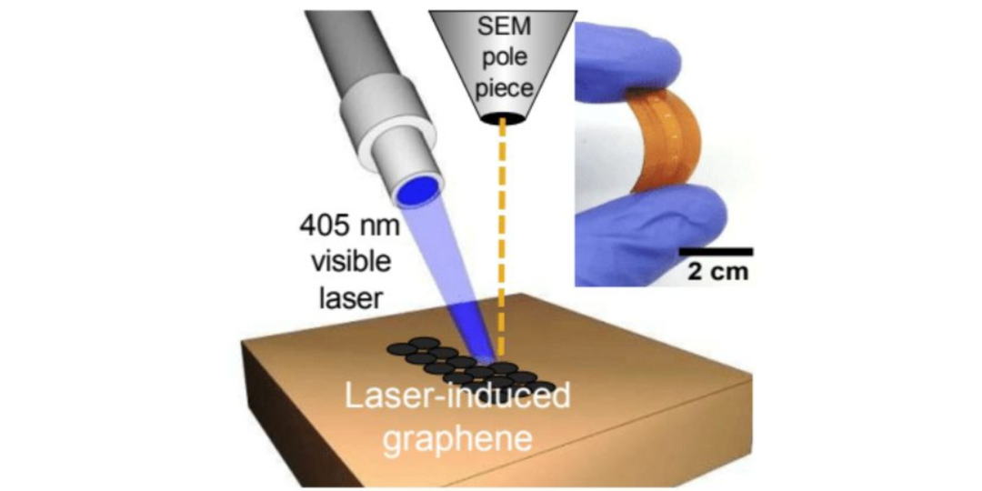
Vesta Desktop SEM
Compatible with all desktop SEM models with side ports
Can co-exist with eds, EBSD and EBIC detectors
Auto-Optical Focus
“Aimed” fast and intuitive laser alignment
Fully integrated Python software development kit
Raman, CL, PL, heating in situ
Tailored solution
Extreme Ultra High Vacuum Compatible (10-10 Torr)
Supports bakeable system requirements
Compatible with all vacuum systems with suitable ports
Optimized for EUV and IR laser sources
TEM, SEM/FIB, desktop SEM gas injection capability
Fully customized to the needs of the application
Argon ion beam sampling
Hungarian Technoorg Linda ion grinder, ion finishing instrument, ion thinning instrument, using ion beam technology, can quickly grind samples, surface finishing and final polishing. It is a powerful tool for surface treatment of SEM/TEM samples.
Technoorg Linda provides argon ion sampling solutions covering SEM and TEM analysis processes for mechanical grinding scratches, surface deformation and ion beam sampling damage in materials, devices and packaging analysis.
Recommended model
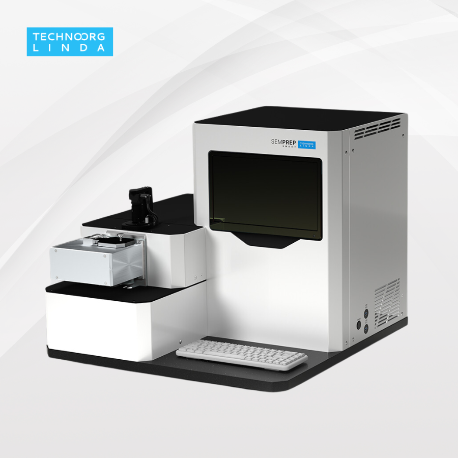
Benchtop ion grinder smart
Designed for surface fine polishing and cross-sectional preparation of SEM samples. By regulating the argon ion beam to remove the stress deformation layer and damage scratches left by mechanical grinding, the real microphysical structure of led contacts, package solder balls, and multi-layer heterojunction interfaces such as Si/SiGe and GaN can be clearly presented, providing a high-fidelity cross-section for semiconductor process evaluation and failure analysis (FA).
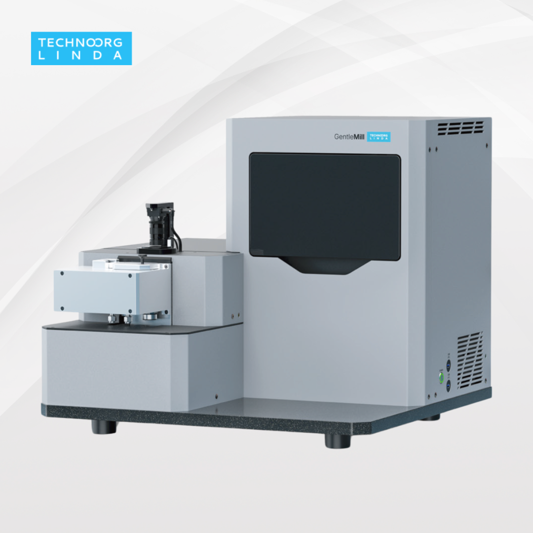
Benchtop Ion Finishing Instrument Gentle Mill
Focus on high quality TEM/stem sample preparation. In response to the surface amorphization and ion implantation damage caused by FIB (focused ion beam) processing of semiconductor sheets, Gentle Mill uses low-energy argon ions as low as tens of electron volts for secondary cleaning and ultimate thinning, effectively removing the non-crystalline layer, and providing high-quality non-destructive samples for atomic-level high-resolution TEM observation and eels analysis of wide bandgap semiconductors.
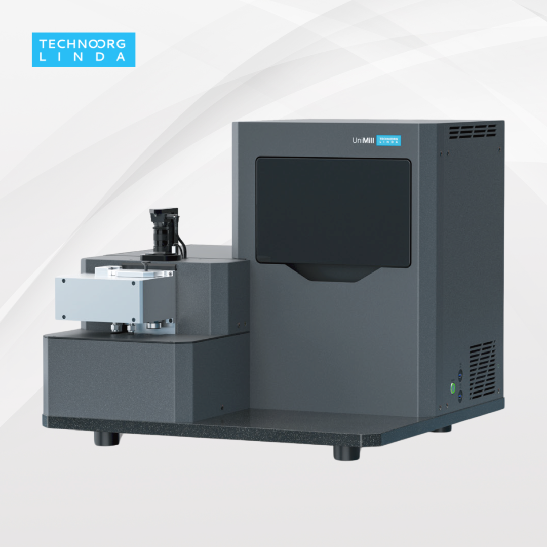
Benchtop Ion Thinning Instrument Unimill
An all-purpose ion sampling platform that combines large-area high-uniformity thinning of TEM sheets with fine-polishing of micro-areas. Suitable for the rapid and efficient thinning of high hardness materials of third/fourth generation wide bandgap semiconductors (SiC, Ga ₂ O ², diamond, etc.), it can thin hard substrates and eliminate the crystal stress distribution in a very short time, laying a good sample foundation for the analysis of microscopic defects and dislocation density of power semiconductor devices and epitaxial materials.
Application cases
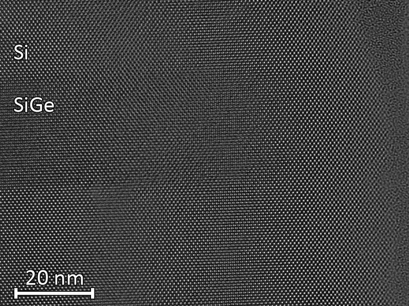
Si/SiGe multilayer structure: after low energy milling
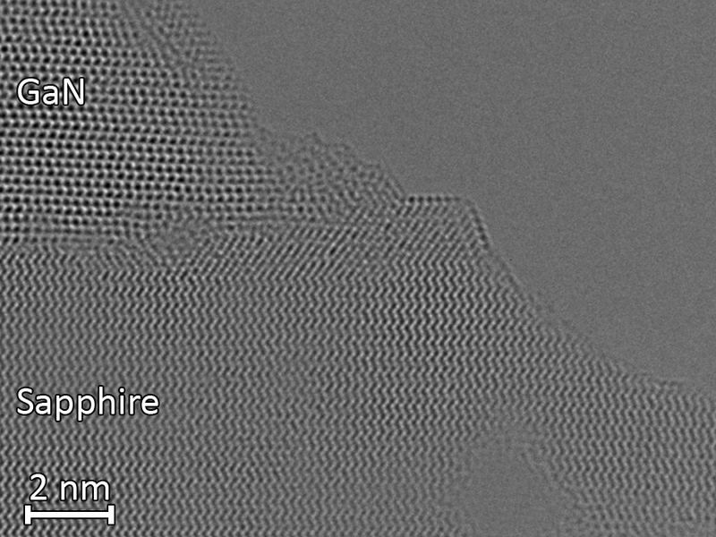
GaN/Sapphire: Highly refined
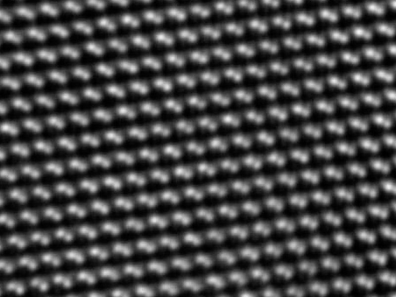
Silicon atom resolution: automatic thinning
Upcoming Booth Events
Workshop Speakers & Schedule

Kimberly Shih
Delmic Sales Manager
SPARC Spectral 3.0 Cathodoluminescence Technology and Application Reveal
Time: October 17th 10:00 - 10:30
October 18th 15:00 - 15:30
Location: Core 2-4 Unbounded Booth

Marek Jemelka
Sales & Marketing Manager, NenoVision
AFM-IN-SEM, Pioneering New Solutions for In-situ Microscopic Characterization
Time: 15:00 - 15:30, October 17th
October 18th 10:00 - 10:30
Location: Core 2-4 Unbounded Booth
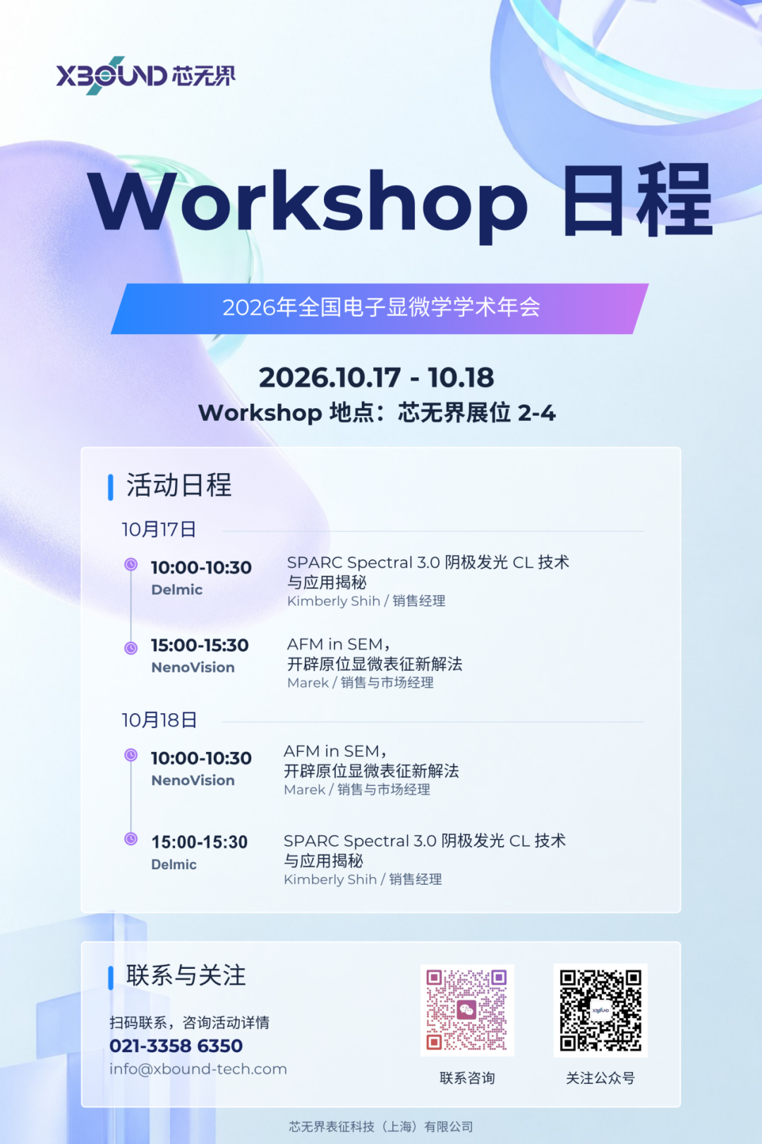
Workshop Schedule

Live Interaction · Fine Gifts
XBOUND Booth Number
2F T4
While experiencing the richness of Xin Boundless products, we also prepared a series of fun and interesting activities for everyone! Welcome everyone to the 2nd floor [2-4] booth to actively participate in the interaction! Live Draw!

Chapter Punch · Zero Dollar Draw
Fill in the questionnaire and get a stamped passport on site
to enter the lottery!
You won 100% of the prize!
October 16th - 20th, Nanjing Buckingham Hotel booth 2-4, look forward to your teachers and industry colleagues to come and guide, let's face-to-face talk about your new needs!
Consultation Hotline: 021-3358 6350 | E-mail:info@xbound-tech.com
XBOUND Characterization Technology is committed to exploring the microscopic world boundaries, focusing on advanced electron microscopy and multi-dimensional characterization technology. Through innovative instrument platforms and professional solutions, electronic microscopy, in-situ analysis, photoelectric correlation and intelligent characterization technologies are connected, providing unlimited possibilities for scientific research and industrial innovation.At present, we mainly provide the following products: advanced SEM/TEM accessories such as Delmic cathodoluminescence in the Netherlands, NenoVision electron microscope atomic force microscope in the Czech Republic, and Waviks in-situ laser heating and light excitation system in the United States. At present, there is a demo experience center in Shanghai, and after-sales service covers the whole country.


Scan the code to focus on "XBOUND Characterization Technology"
 021-3358 6350