



Invitation | Meet XBOUND at APWS 2026 in Xi'an
 |  |
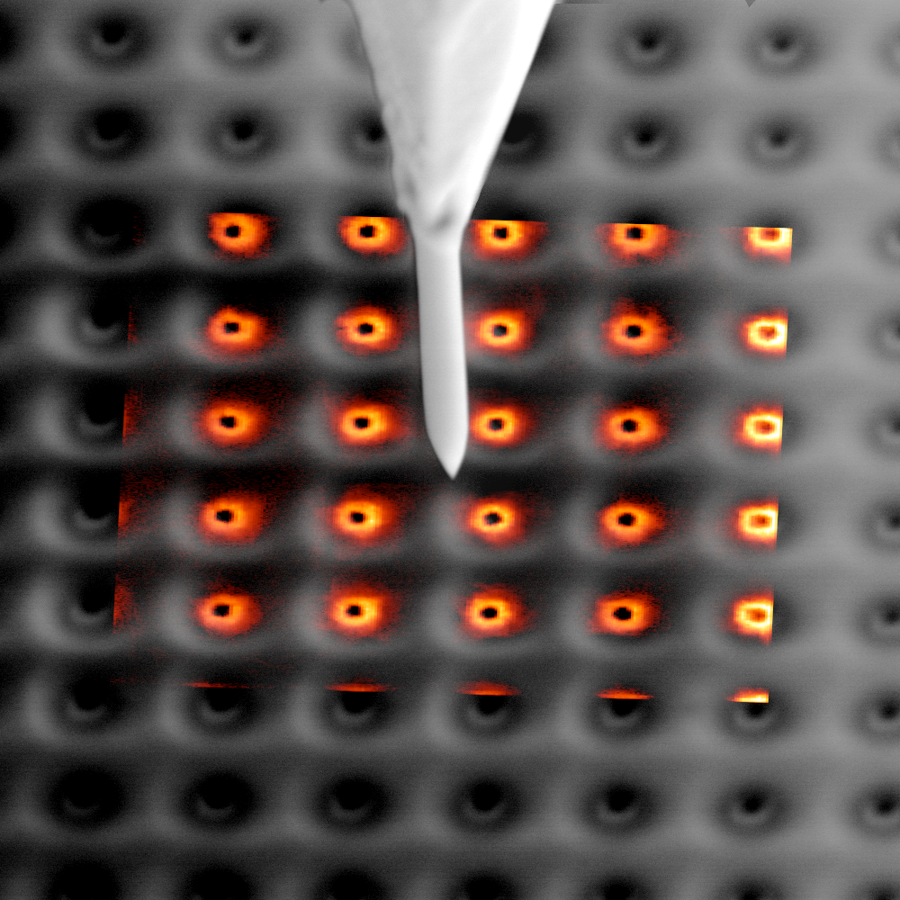 | 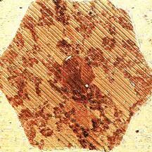 |
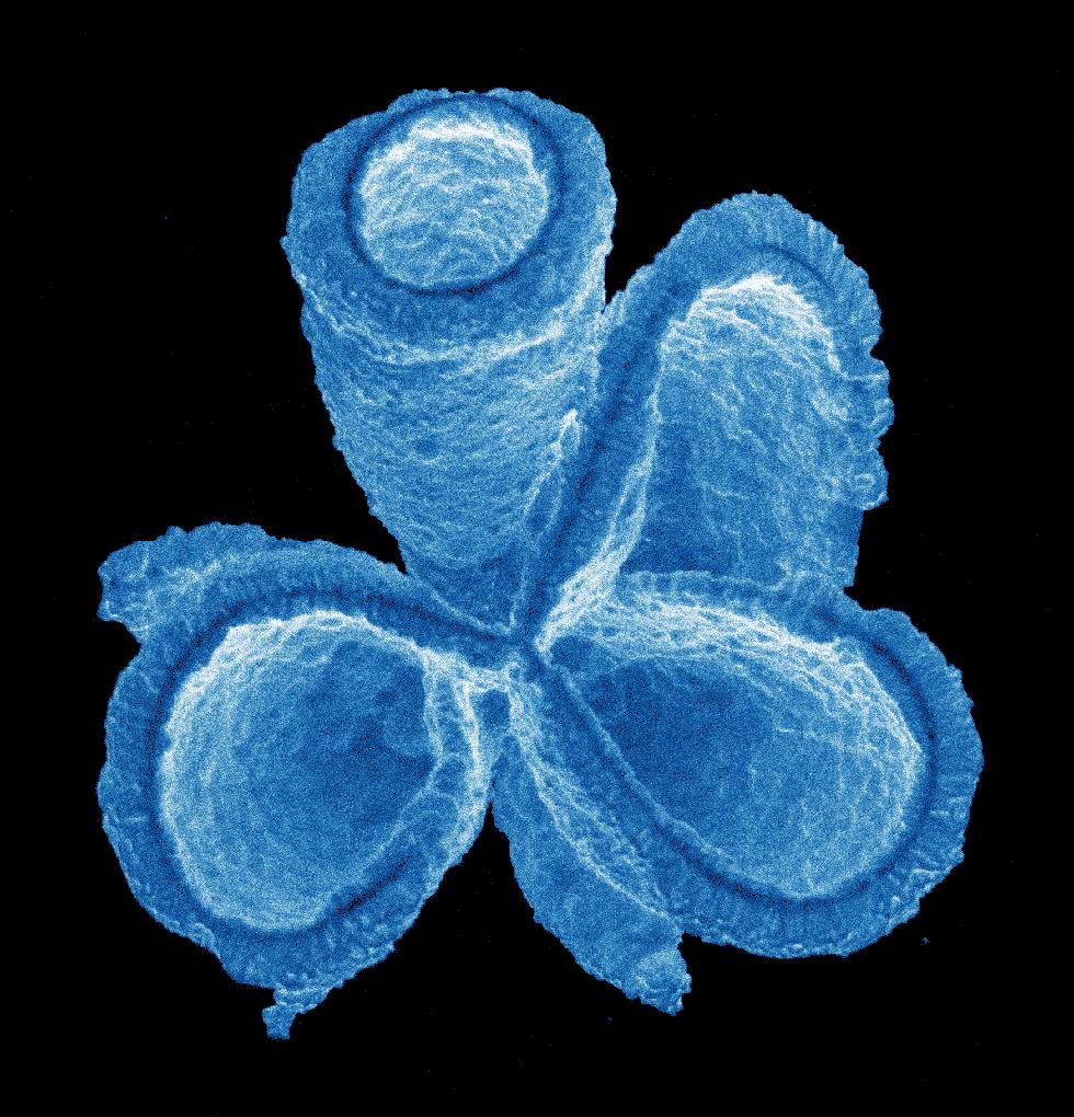
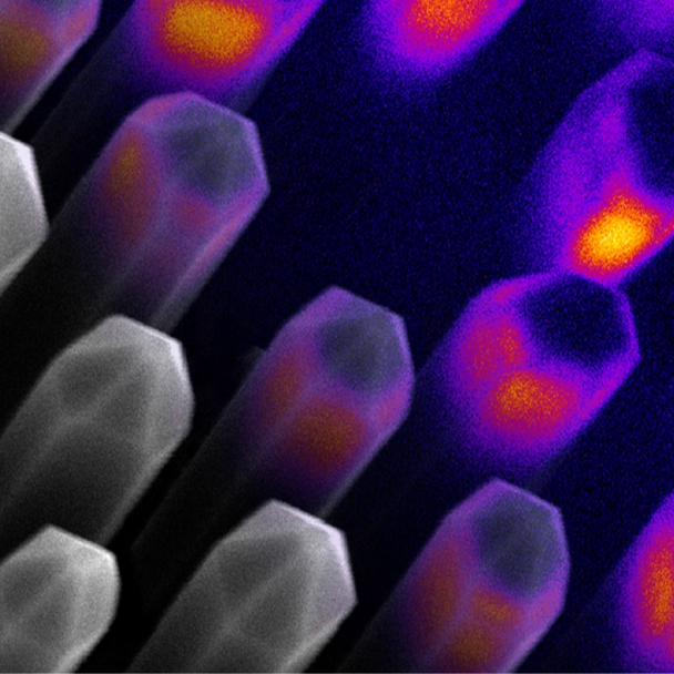
What else can we read from the material after seeing the microstructure? From local luminescence to surface morphology, from static observation to in-situ analysis within an electron microscope, the characterization of different dimensions provides more clues for understanding materials.
On October 11—15, 2026, the 12th Asia-Pacific Broadband Ban Semiconductor Conference (APWS 2026) was hosted by Xi 'an University of Electronics and Technology and will be held in Xi 'an. XBOUND XBOUN
Bring your research questions to A16
Whether you are looking at local differences in materials or want to establish associations between multiple characterization results, you are welcome to share your samples, existing platforms, and research objectives with us. Let the conversation begin with a specific question, looking for a more appropriate representation path.
Session:11-15 October 2026
Venue:China · Xi 'an · Qujiang International Hotel
Booth:A16
Contact:021-3358 6350|info@xbound-tech.com
Registration:www.apws2026.com/signin
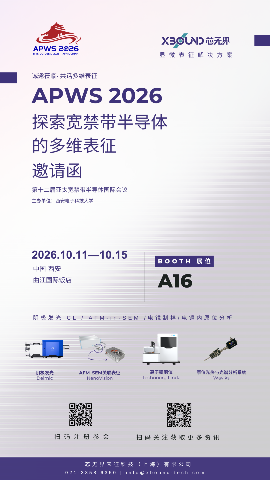
Invitation to the 12th Asia Pacific Broadband Banning Semiconductor Conference (APWS 2026) · Xi 'an · Booth A16
XBOUND products
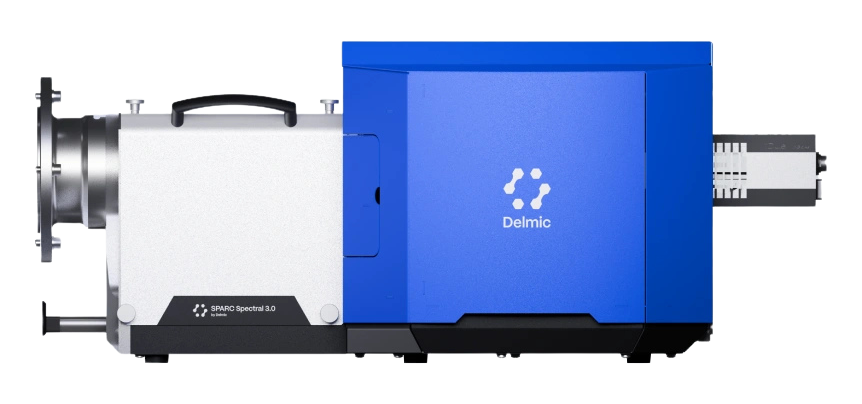
Delmic Cathodoluminescence
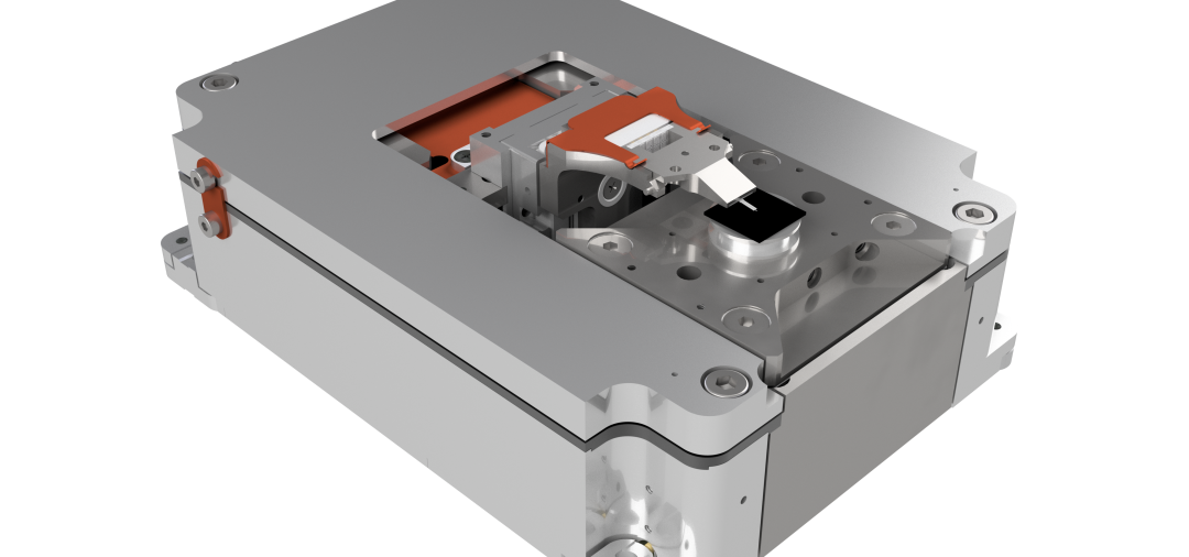
AFM Electron Microscope Atomic Force Microscope
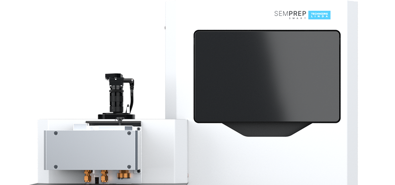
Technoorg Linda Ion Grinder
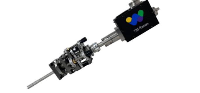
Waviks in-situ photothermal and spectroscopic analysis system
Consultation Hotline: 021-3358 6350 | E-mail:info@xbound-tech.com
XBOUND Characterization Technology is committed to exploring the microscopic world boundaries, focusing on advanced electron microscopy and multi-dimensional characterization technology. Through innovative instrument platforms and professional solutions, electronic microscopy, in-situ analysis, photoelectric correlation and intelligent characterization technologies are connected, providing unlimited possibilities for scientific research and industrial innovation.At present, we mainly provide the following products: advanced SEM/TEM accessories such as Delmic cathodoluminescence in the Netherlands, NenoVision electron microscope atomic force microscope in the Czech Republic, and Waviks in-situ laser heating and light excitation system in the United States. At present, there is a demo experience center in Shanghai, and after-sales service covers the whole country.

Scan the code to focus on "XBOUND Characterization Technology"
 021-3358 6350