




Introducing the Next-Generation SPARC Spectral 3.0 Cathodoluminescence System
 |  |
 |  |
Cathodoluminescence (CL) Solution
As a "deep-seated and accurate" microscopic characterization tool in the fields of materials science, semiconductors, and nanophotonics, cathodoluminescence (CL) technology has long faced application bottlenecks such as "high threshold, dependence on expert experience, and long scanning time".
The release of SPARC Spectral 3.0 is rewriting that.
At the 21st International Microscopy Congress (IMC21) in Liverpool, Dutch characterization equipment giant Delmic officially launched a new generation of flagship cathodoluminescence system, SPARC Spectral 3.0, to the world. It continues Delmic's iconic modular design while leapfrogging hardware speed, software automation, and multimodal correlation capabilities - from “expert proprietary tools” to “high-throughput, automatable, and more user-friendly” analytics platforms.
01| SPARC 3.0 Core Benefits:
Enabling nanoscale optical characterization: higher flux, greater stability, lower threshold of use.
Simplify workflows - one-click auto alignment, auto raster calibration
Significantly increased throughput - 2.3x faster hyperspectral scanning
Unlock linkage characterization - CL and PL together, FIB-SEM seamless switching
Future-proof upgradeable - modular body to support on-site installation of new modules
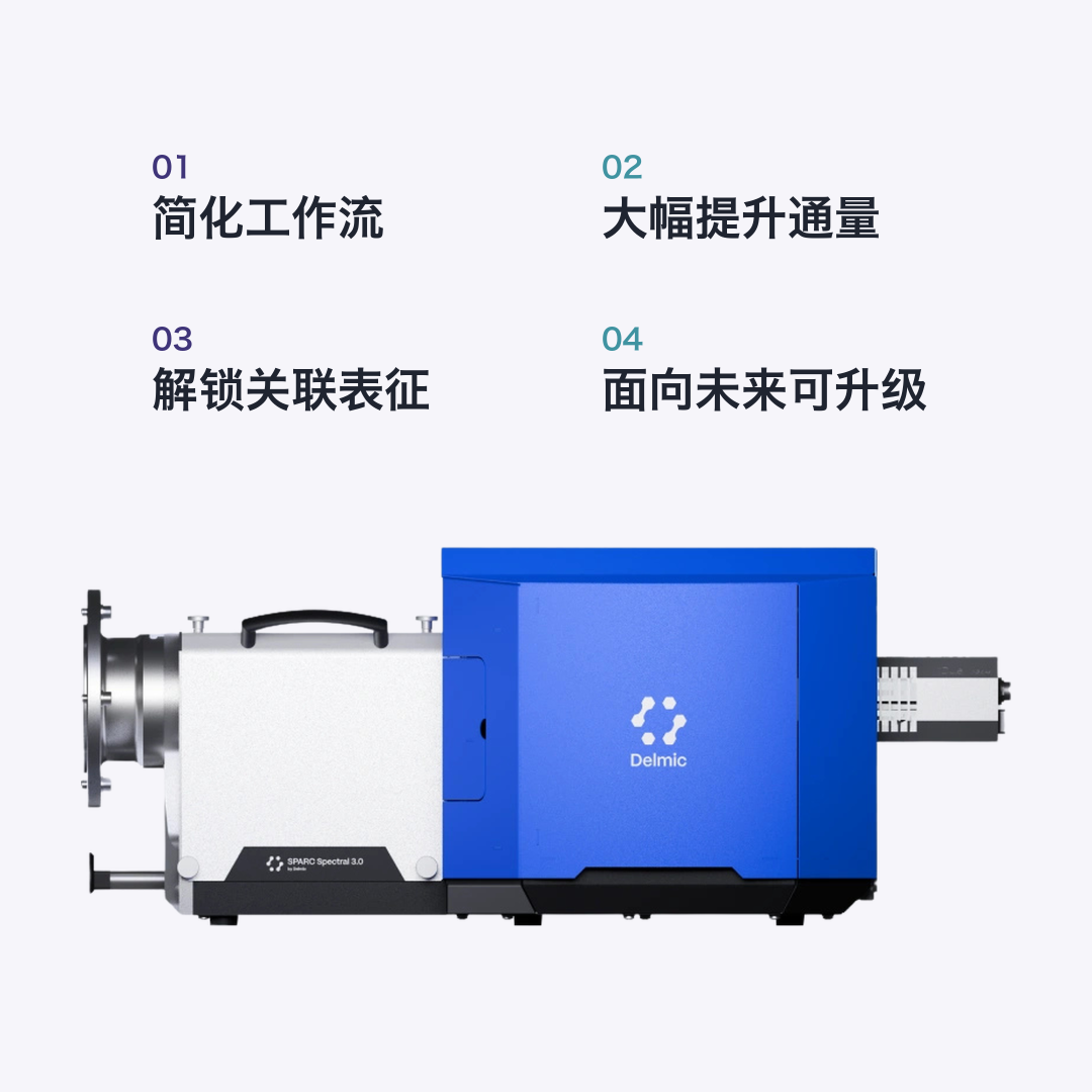
SPARC Spectral 3.0 Four Core Benefits
02| Hardware Highlights
SPARC SPECTRAL 3.02.3x faster hyperspectral scanning
CCD hardware triggered, 128 × 128 pixel scan reduced from 15.4 minutes to 6.5 minutes. Beam-sensitive samples can be scanned for higher resolution before degradation.
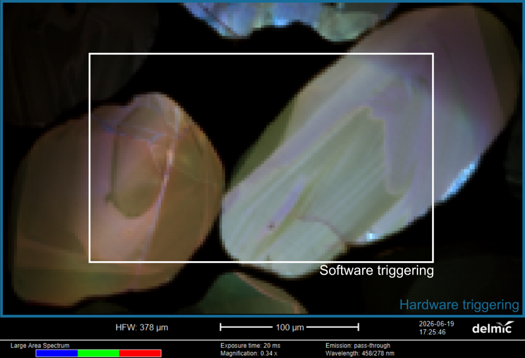
ODEMIS software acquisition interface (CCD hardware trigger)
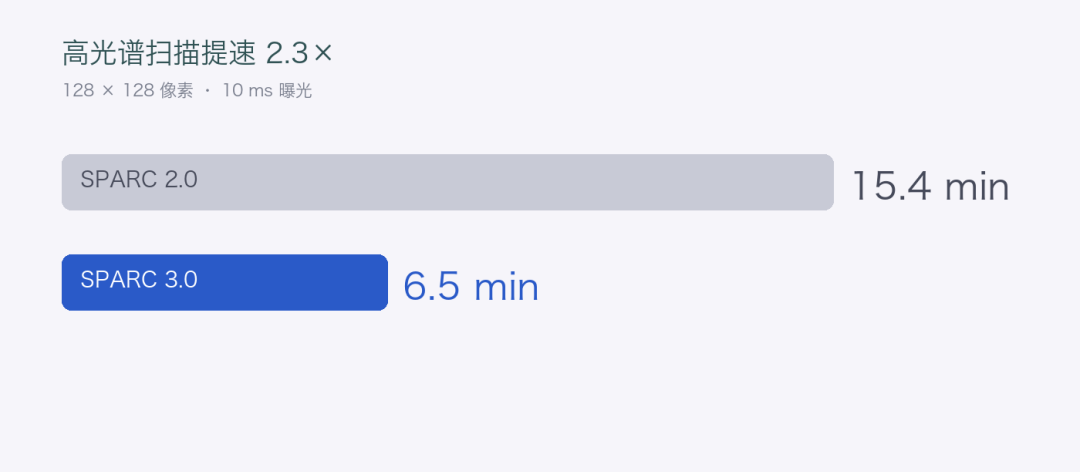
Hyperspectral scan speed-up: 15.4 minutes → 6.5 minutes
SPARC SPECTRAL 3.0
Up to three lasers (405/532/633 nm) are injected into the SEM cavity to achieve CL + PL nanoscale correlation under the same vacuum environment. Sensitive materials such as perovskites, organic semiconductors, etc. do not need to transfer samples between multiple instruments.
SPARC SPECTRAL 3.0Monochromated Photon Count PMT
Microsecond dwell time + subnanometer spectral selectivity, suitable for microLED defect screening and high-throughput quantitative mapping of specific wavelengths.
SPARC SPECTRAL 3.04 mm short working distance mirror
Compatible with FIB-SEM concentric points, CL characterization and FIB processing switching are smoother; low-voltage SEM imaging performance is better.
SPARC SPECTRAL 3.0Body and Stagebox Reconfiguration
The positioning accuracy of the Stagebox is 1.2 μm, and the retraction speed of the mirror is increased to 6 mm/s (4 times); the blind flange design supports on-site upgrading of PL modules, Lab Cube, etc.
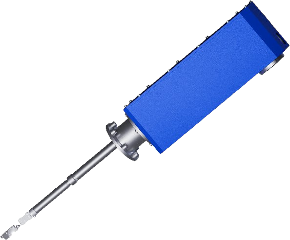
PL module in situ (FPLM)
03| Software Highlights (ODEMIS)
| Function | Value |
|---|---|
| One-click 3D mirror auto alignment | ~ 5 minutes to complete X/Y/Z alignment, eliminate operator differences |
| Automatic raster calibration | Zero-order diffraction peak is centered at < 0.4 pixels, consistent across session data |
| Arbitrary Shape & Multiple ROI | Fit zircon grain, round microLED, support overnight unattended |
| Intelligent stitching collection | Large wafer/geological mount automatic Z height compensation with consistent focus |
| Acquisition formula | Experimental parameter export/import to ensure repeatability |
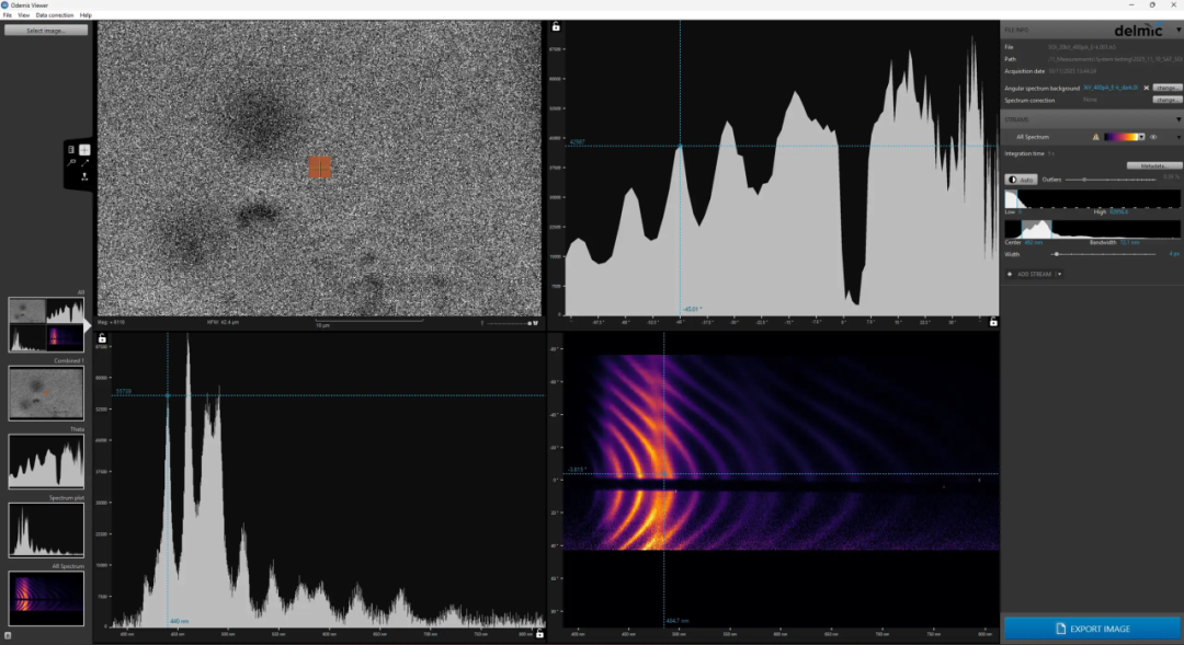
Overview of ODEMIS Software Features
| Configure | Typical Applications |
|---|---|
| Spectral B | Geology, Universal Materials, Platform Sharing (UV-NIR Broad Spectrum) |
| Spectral U | Wide bandgap materials, UVC LEDs, power electronics |
| Spectral V | Nanophotonics, microLEDs, perovskites, 2D materials |
| Spectral R | Large wafer/geological mount automatic Z height compensation with consistent focus |
Use Case Demonstration
Delmic Cathodoluminescence Technology Series Products
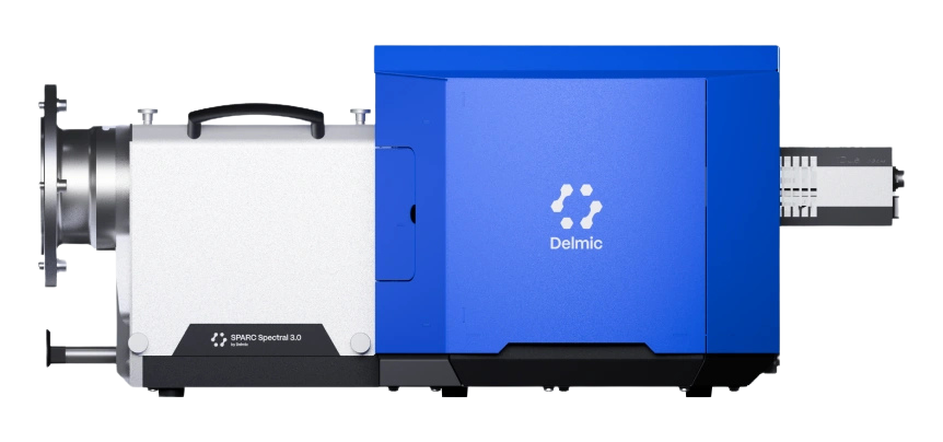
SPARC Spectral 3.0
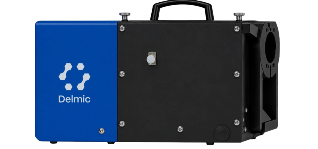
SPARC Compact
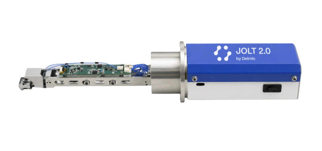
JOLT
Consultation Hotline: 021-3358 6350 | E-mail:info@xbound-tech.com
XBOUND Characterization Technology is committed to exploring the microscopic world boundaries, focusing on advanced electron microscopy and multi-dimensional characterization technology. Through innovative instrument platforms and professional solutions, electronic microscopy, in-situ analysis, photoelectric correlation and intelligent characterization technologies are connected, providing unlimited possibilities for scientific research and industrial innovation.At present, we mainly provide the following products: advanced SEM/TEM accessories such as Delmic cathodoluminescence in the Netherlands, NenoVision electron microscope atomic force microscope in the Czech Republic, and Waviks in-situ laser heating and light excitation system in the United States. At present, there is a demo experience center in Shanghai, and after-sales service covers the whole country.


Scan the code to focus on "XBOUND Characterization Technology"
 021-3358 6350