



Explore the Microscopic World of Light: A Guide to Cathodoluminescence (CL)
 |  |
 |  |
Cathodoluminescence (CL) Solution
01| What is cathodoluminescence?
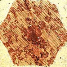
Cathodoluminescence (CL) is light or electromagnetic radiation in the ultraviolet (UV) to near infrared (NIR) range of electromagnetic waves produced by the fast electrons (cathodoluminescence) of an electron beam.
Various processes occur when an electron beam (e.g. from a scanning electron microscope) interacts with a material (bulky, thick, or thin), and these processes can be used for a variety of microscopic observations. In addition to electronic signals, various incoherent and coherent processes generate a wide range of electromagnetic radiation.
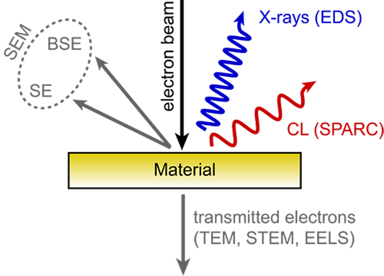
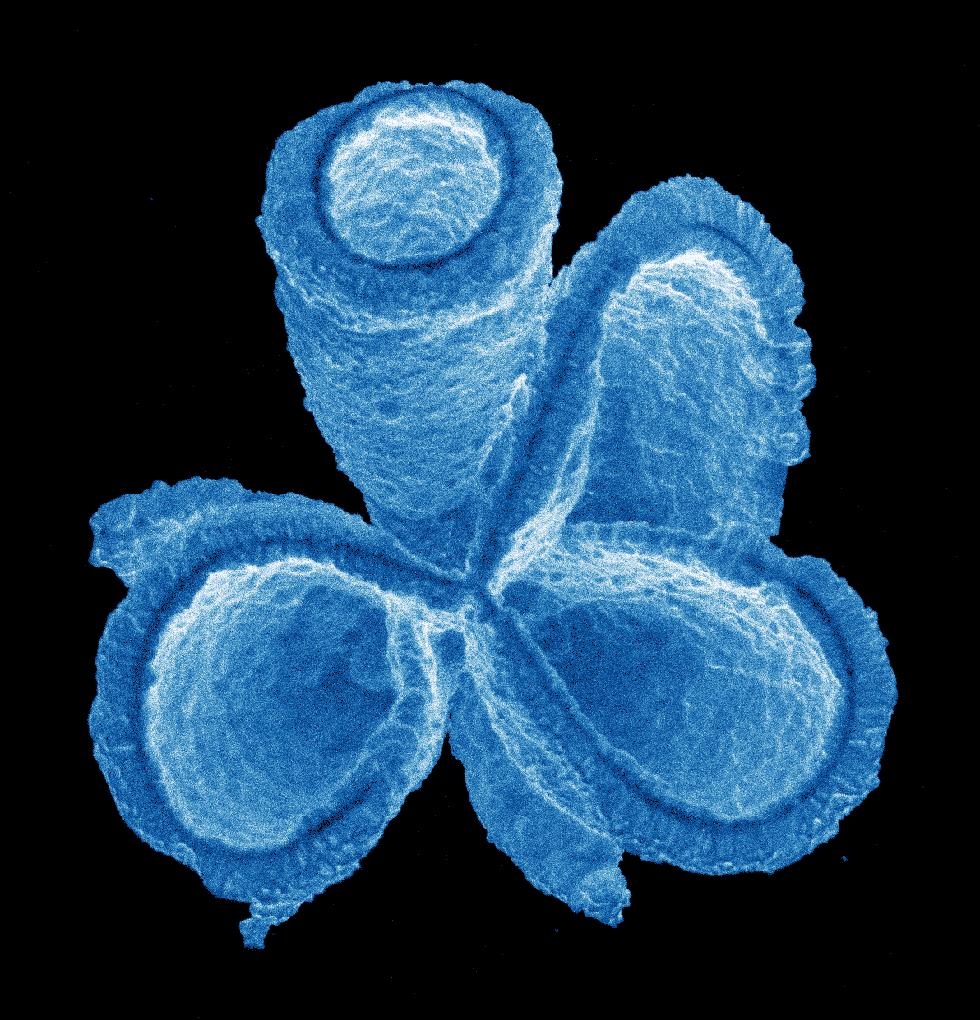
Schematic diagram of cathodoluminescence mechanism
02| How to image cathodoluminescence?
Cathodoluminescence technology is typically implemented based on scanning electron microscopy (SEM). The sample is excited by the focused electron beam in a vacuum environment, which generates a cathodoluminescent signal, providing important information for the analysis of the microscopic optical properties of the material.
Signal Acquisition and Detection Process
The light generated by the sample under the action of the electron beam must be collected with a collection optic (such as a mirror or objective) or directly captured by a cathodoluminescent detector within the chamber.
When light is collected through an optical element, it is directed to a light detection element, such as a photomultiplier tube (PMT), a spectrometer, or a camera.
The Delmic SPARC spectrometer is one such detector that can be adapted into any scanning electronic system (SEM) to produce high-performance cathodoluminescent images. The unique advantages of cathodoluminescence detection are its ease of operation and the highly optimized efficiency of cathodoluminescence signal collection and detection.
03| CL vs. other SEM technologies
Here's how common electron microscopy techniques compare to cathodoluminescence:
| Name of technology | TEST PRINCIPLE | Information available |
|---|---|---|
| Secondary electron (SE) testing | Detect low energy electrons | It is sensitive to surface topography and also displays (smaller) material contrast, collecting signals from only a few nanometers at the top of the material |
| Backscatter electron (BSE) detection | Detect backscattered electrons | Mainly sensitive to density and atomic number, it can be used to obtain material contrast |
| Electron Backscatter Diffraction (EBSD) | Analyze the diffraction pattern of backscattered electrons | View crystal structure and crystal orientation |
| Energy Dispersive X-ray Spectroscopy (eds) | Detecting Nuclear Transitions in Materials | Can be used for quantitative elemental analysis |
Complementary benefits of cathodoluminescence
The emission energy range of 0.5 to 6 eV can be observed, covering many important physical processes, and information on composition, crystal structure and electron bandgap can be obtained.
It can sensitively detect trace elements or dopants, can also be used to view crystal defects, and can also image optical resonance and guidance modes in (resonant) photon and plasma systems.
In combination with other electron microscopy-based techniques, very complete material analysis can be performed and can also be used as a pre-screening tool for more time-consuming and expensive techniques such as mass spectrometry for quantitative isotope analysis.
04| What data can be obtained using cathodoluminescence?
Different imaging modes of cathodoluminescence can provide new insights and information layers for the sample, the six most commonly used imaging modes are as follows:
Rapid intensity imaging
Rationale:Large-scale imaging using rapid photomultiplier tube (PMT) detectors enables rapid detection of large areas and efficient searching of areas of interest. The filter wheel built into the system can be used for spectral differentiation.
APPLICATIONS:Ideal for mineralogical applications such as observing zoning and overgrowth.
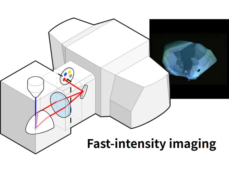
Rapid intensity imaging mode
Hyperspectral Camera
Rationale:Visually display the wavelength distribution (spectrum) of the material.
APPLICATIONS:Mainly used in (nano) materials, semiconductors, and geological samples (e.g., zircon and quartz sandstone).
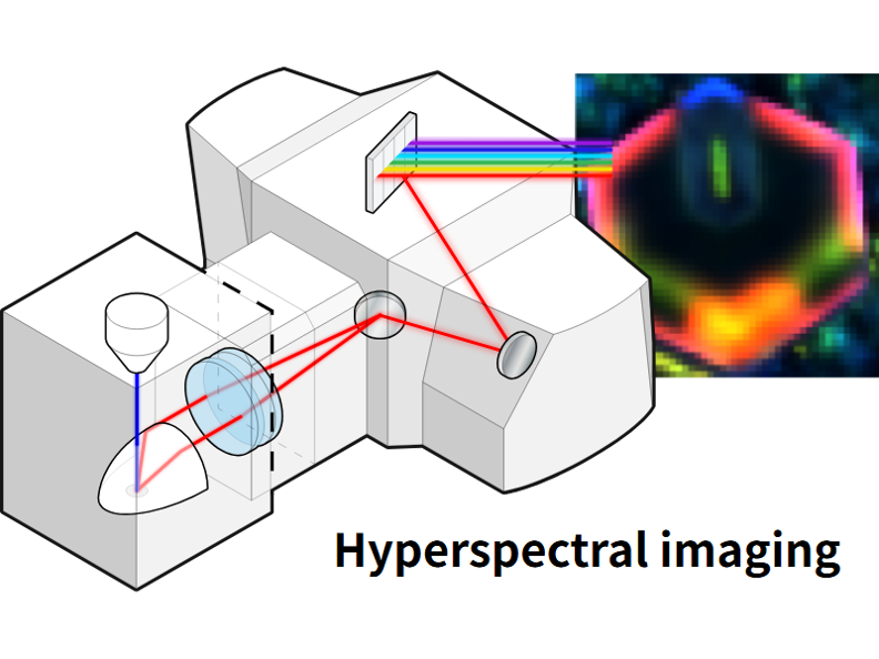
Hyperspectral imaging mode
Angle-resolved imaging
Rationale:Used to study how a sample emits and scatters light by angular resolution of cathodoluminescence. Each point acquired on the image corresponds to a unique emission angle, so we can use it to characterize the properties of the material.
APPLICATIONS:The angular profile obtained by this imaging mode is very valuable in the field of nanophotonics.
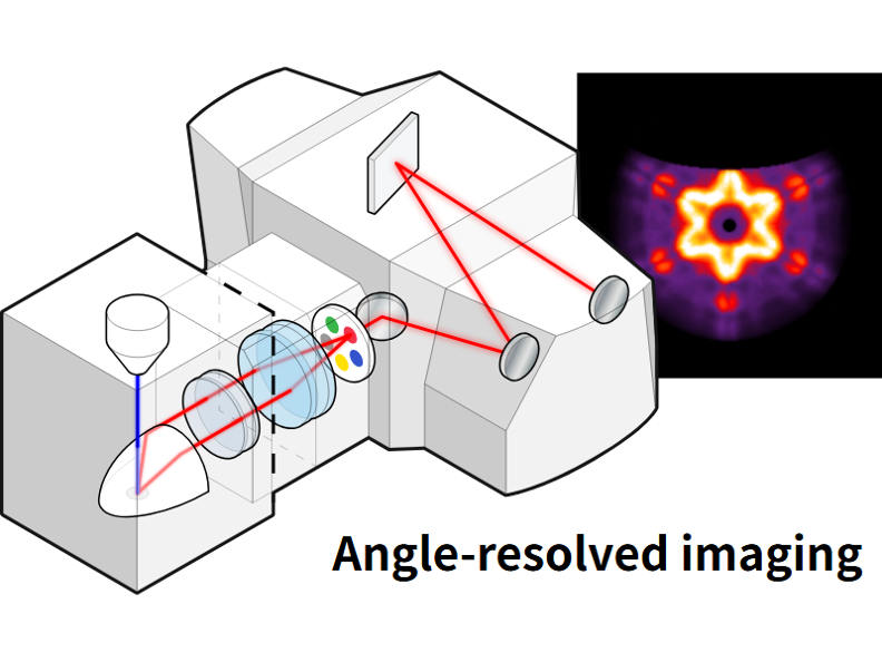
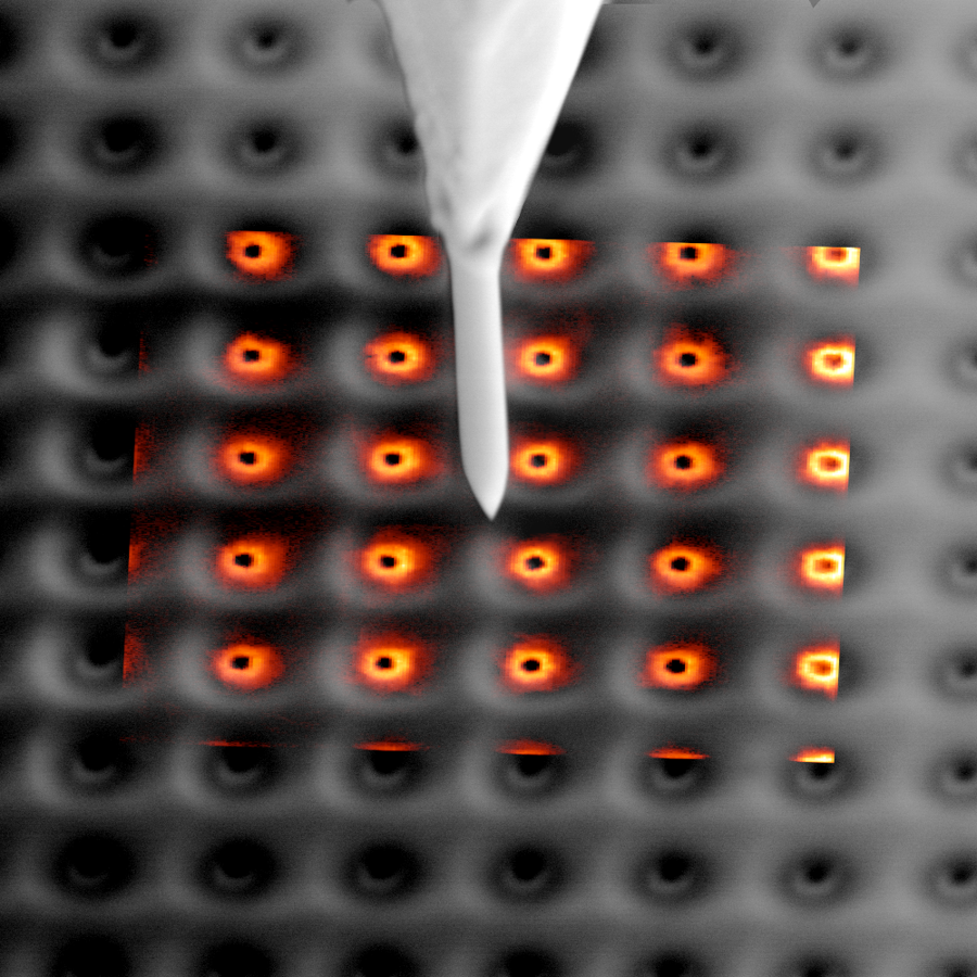
Angle-resolved imaging mode
Polarization and Polarization Filter Spectrum
Rationale:Measuring the polarization of light reveals the direction in which the electromagnetic field oscillates. This technique allows the polarization state (Stokes vector) of the cathodoluminescence to be measured for different emission angles.
APPLICATIONS:Can be used for comprehensive measurements of coherence, scattering and chirality.
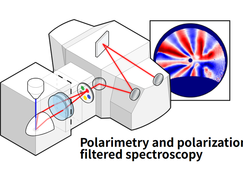
Polarization and Polarization Filtering Spectral Modes
Lens scanning energy momentum (LSEK) imaging
Rationale:For any given location on the sample, this mode captures high-resolution datasets with resolved angles and wavelengths. Lens scanning energy momentum imaging mode can track and characterize the optical properties of nanomaterials through highly accurate energy momentum space.
APPLICATIONS:Can be applied to a variety of dispersive and anisotropic (photonic) systems, paving the way for extensive research in applications such as solid-state lighting, photovoltaics, and sensing.
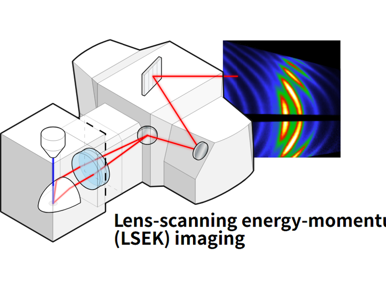
Lens scanning energy momentum (LSEK) imaging mode
Time-resolved cathodoluminescence imaging
Rationale:Photon lifetime detection and g (2) imaging using the optional Lab Cube time resolution module. Delmic's Lab Cube is the only product on the market that can be used to perform anti-binding experiments and characterize nanoscale single-photon emitters.
APPLICATIONS:Closely related to a wide range of applications, including semiconductors for photovoltaics, light-emitting devices, and (single) emitters for quantum information processing and sensing.
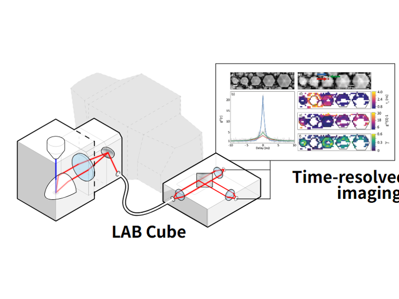
Time-resolved cathodoluminescence imaging mode (Lab Cube)
05| How to apply cathodoluminescence to research?
Cathodoluminescence, with its sensitivity to a range of basic processes in materials, ease of use and high spatial resolution, is a very useful microscopic technique that can analyze the properties of materials over a very small length range. Its main application areas are as follows:
Nanophotonics
Suitable for metal as well as dielectric and semiconductor nanostructures including nanoparticles, nanowires, supramolecular, supersurface and photonic crystals. These structures can be used in the fields of (biological) sensing, fluorescence enhancement, nonlinear optics, low-threshold steam generation, LEDs, solar cells, integrated photonics, lasers, etc.
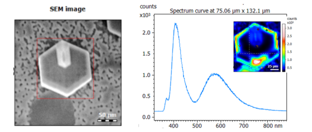
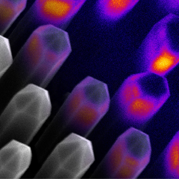
Nanowire led
Geological Sample Study
Cathodoluminescence (CL) is an ideal tool for studying geological samples and obtaining additional contrast and spectral information down to scanning electron microscope resolution. The cathodoluminescence emitted by the rocks provides insight into information about crystal growth, banding, cementation, displacement, deformation, provenance, trace elements, and defect structures. Can be used to fingerprint rocks and display interesting spatial textures at the submicron level.Often used in conjunction with other analytical tools, such as Sims, LA-ICP-MS, BSE, eds, WDS, and μCT, for a more comprehensive understanding of all relevant rock properties.
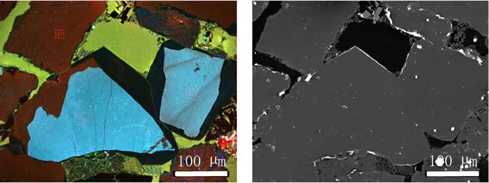
RGB CL strength of quartz sandstone (left) and SE image (right)
Research on ceramics, dielectrics and (compounds) semiconductors
Such materials play an important role in many devices and functional materials, including scintillators, phosphors, high-power electron light emitting diodes, diode lasers, and solar cells. Nanostructuring is increasingly used to optimize the optical properties of these materials. Cathodoluminescence can be used to study these materials (bulk and nanostructured materials) and determine their luminescence properties at the nanoscale.
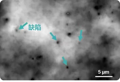
CL Intensity Diagram for InGaN Multi-Quantum Wells
Soft Matter Field
Increasingly used in soft materials, including polymers and biological tissues.
06| Sample preparation for cathodoluminescence
The sample preparation process for cathodoluminescence is not very complicated, the main steps are as follows:
Check that the sample is vacuum compatible. If the surface is dirty, it can be assisted by chemical cleaning or reactive ion etching.
Check that the sample surface is flat enough. Avoid large differences (> 0.1 mm).
The sample must have sufficient electrical conductivity to prevent charging effects in the electron microscope. To do this, it is good to coat the sample with a thin layer of carbon or metal. Low vacuum mode imaging available in some electron microscopes can mitigate the charging effect.
Differences in preparation of different materials
Geological materials:The most commonly used preparation techniques are slicing (20 to 30 microns) or resin embedding.
Artificial materials (e.g. semiconductor wafers):Often flat and already electrically conductive, so in most cases no additional preparation is required.
Powder Material:Fix the powder on the carbon tape and coat it with carbon or metal if needed.
Important notes:These steps are also required for the preparation of samples for conventional electron microscopy imaging, so cathodoluminescence imaging does not require any additional sample preparation work on the electron microscopy imaging samples.
Delmic Cathodoluminescence Technology Series Products
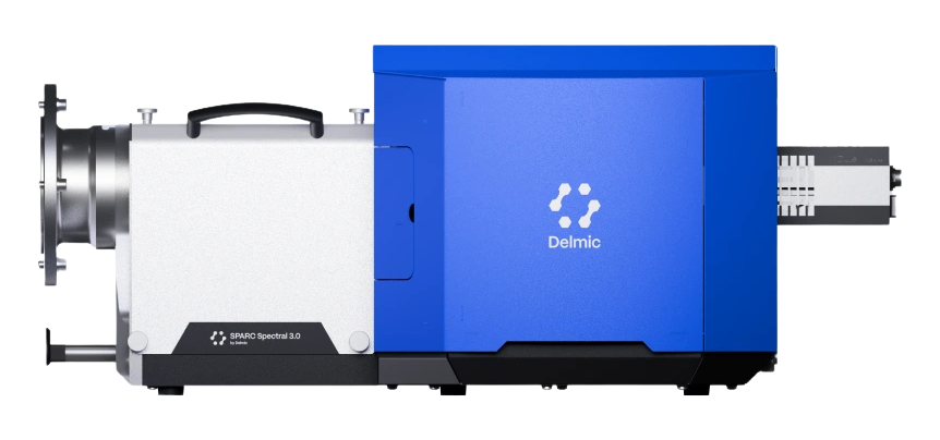
SPARC Spectral
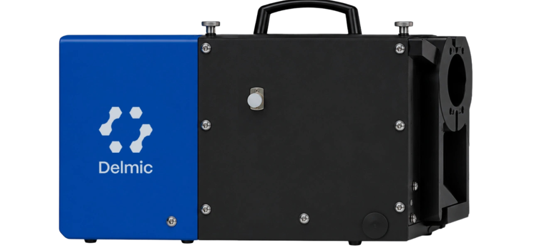
SPARC Compact
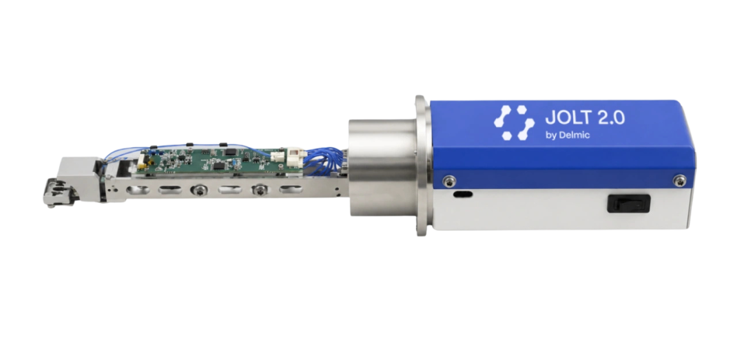
JOLT
Hotline: 8621-3358 6350
XBOUND Characterization Technology is committed to exploring the microscopic world boundaries, focusing on advanced electron microscopy and multi-dimensional characterization technology. Through innovative instrument platforms and professional solutions, electronic microscopy, in-situ analysis, photoelectric correlation and intelligent characterization technologies are connected, providing unlimited possibilities for scientific research and industrial innovation.At present, we mainly provide the following products: advanced SEM/TEM accessories such as Delmic cathodoluminescence in the Netherlands, NenoVision electron microscope atomic force microscope in the Czech Republic, and Waviks in-situ laser heating and light excitation system in the United States. At present, there is a demo experience center in Shanghai, and after-sales service covers the whole country.


Scan the code to focus on "XBOUND Characterization Technology"
 021-3358 6350